Lead-free hybrid perovskite material electric memory device and preparation method thereof
A technology for electrical storage and devices, which is applied in the field of lead-free hybrid calcium carbon mineral electrical storage devices and its preparation, can solve the problems of complex process, low storage density, and high manufacturing cost, and achieve good storage performance, stable and reliable performance, Flexible performance and reliable effect
- Summary
- Abstract
- Description
- Claims
- Application Information
AI Technical Summary
Problems solved by technology
Method used
Image
Examples
Embodiment 1
[0036] Lead-free hybrid calcium carbide MASnBr 3 The configuration diagram of the precursor solution (5mol / L) is shown in figure 1 , all of the following operations are under nitrogen (N 2 ) in a glove box. Take SnBr 2 (2.785g, 10 mmol) with NH 3 CH 2 ∙HBr (1.12g, 10mmol) powder was dissolved in 2 mL of dimethylformamide (DMF) solution, and stirred at 600 rpm to prepare a 5mol / L precursor solution. The preparation schematic diagram is as follows figure 1 shown.
Embodiment 2
[0038] Sandwich device preparation, the prepared device is Au / MASnBr 3 / ITO / SiO 2 sandwich structure. Before spin-coating the functional layer, SiO 2 / ITO (Indium Tin Oxide) film is first washed with washing powder, then ultrasonicated in deionized water, acetone and ethanol for 30 minutes, washed and dried. Subsequently, the SiO 2 / ITO film was cleaned for 15 minutes and set aside.
[0039] All of the following operations are carried out at room temperature under a nitrogen atmosphere (N 2 ) in a glove box. The speed of the homogenizer is first controlled at 1500 rpm, and the 5mol / L MASnBr is spin-coated for 60 seconds. 3 Precursor solution, use poor solvent toluene to assist precipitation; then spin-coated MASnBr 3 / ITO / SiO 2 The film was heated on a heating platform at 70°C for 30 minutes in order to remove excess solvent and form a uniform and dense film. The preparation schematic diagram is shown in figure 1 As shown, the gold electrode is sputtered using the mas...
Embodiment 3
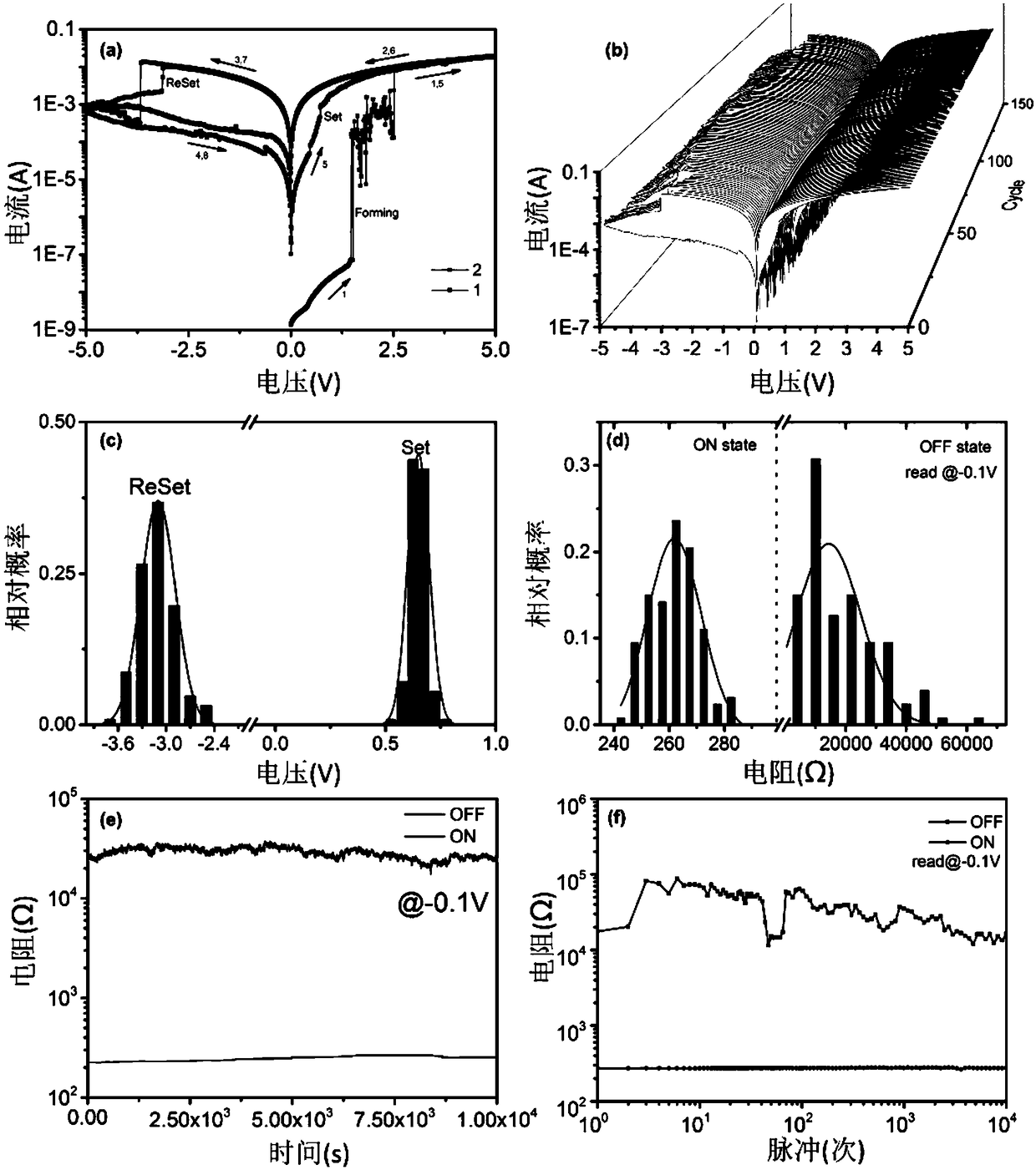
[0042] Memristor, memory capacitive performance test, the Au / MASnBr obtained in embodiment two 3 / ITO / SiO 2 Do I-V performance test, the measured typical curve is as follows figure 2 As shown, (a) the electroforming process and the I-V characteristic curve of the memory device, (b) the 127 continuous cycle I-V curves of the memristive characteristic, (c) the distribution range of the turn-on voltage and the reset voltage, (d) at -0.1 When V is read, the resistance distribution of On / OFF state, (e) When reading at -0.1V, the constant current characteristics of ON / OFF state, (f) in pulse mode, when reading at -0.1V, ON / OFF State durability characteristics; figure 2 It can be shown that the memristive performance of the electric storage device of the present invention has good repeatability and high reliability.
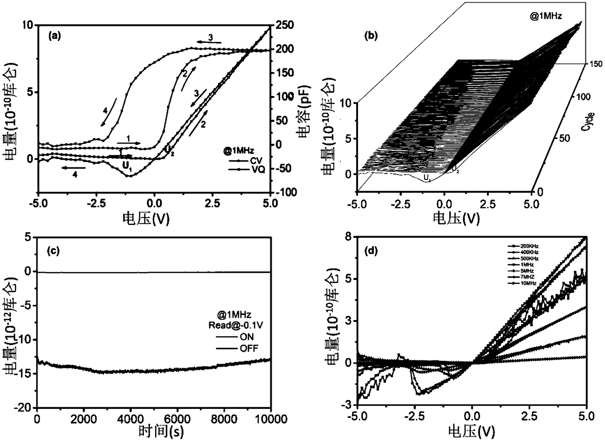
[0043] Obtain Au / MASnBr in embodiment two 3 / ITO / SiO 2 Do C-V, Q-V performance test, the measured typical curves are as follows image 3 As shown, (a) Q-V and C...
PUM
 Abstract
Description
Claims
Application Information
 - R&D Engineer
- R&D Manager
- IP Professional
- Industry Leading Data Capabilities
- Powerful AI technology
- Patent DNA Extraction
Browse by: Latest US Patents, China's latest patents, Technical Efficacy Thesaurus, Application Domain, Technology Topic, Popular Technical Reports.
© 2024 PatSnap. All rights reserved.Legal|Privacy policy|Modern Slavery Act Transparency Statement|Sitemap|About US| Contact US: help@patsnap.com


