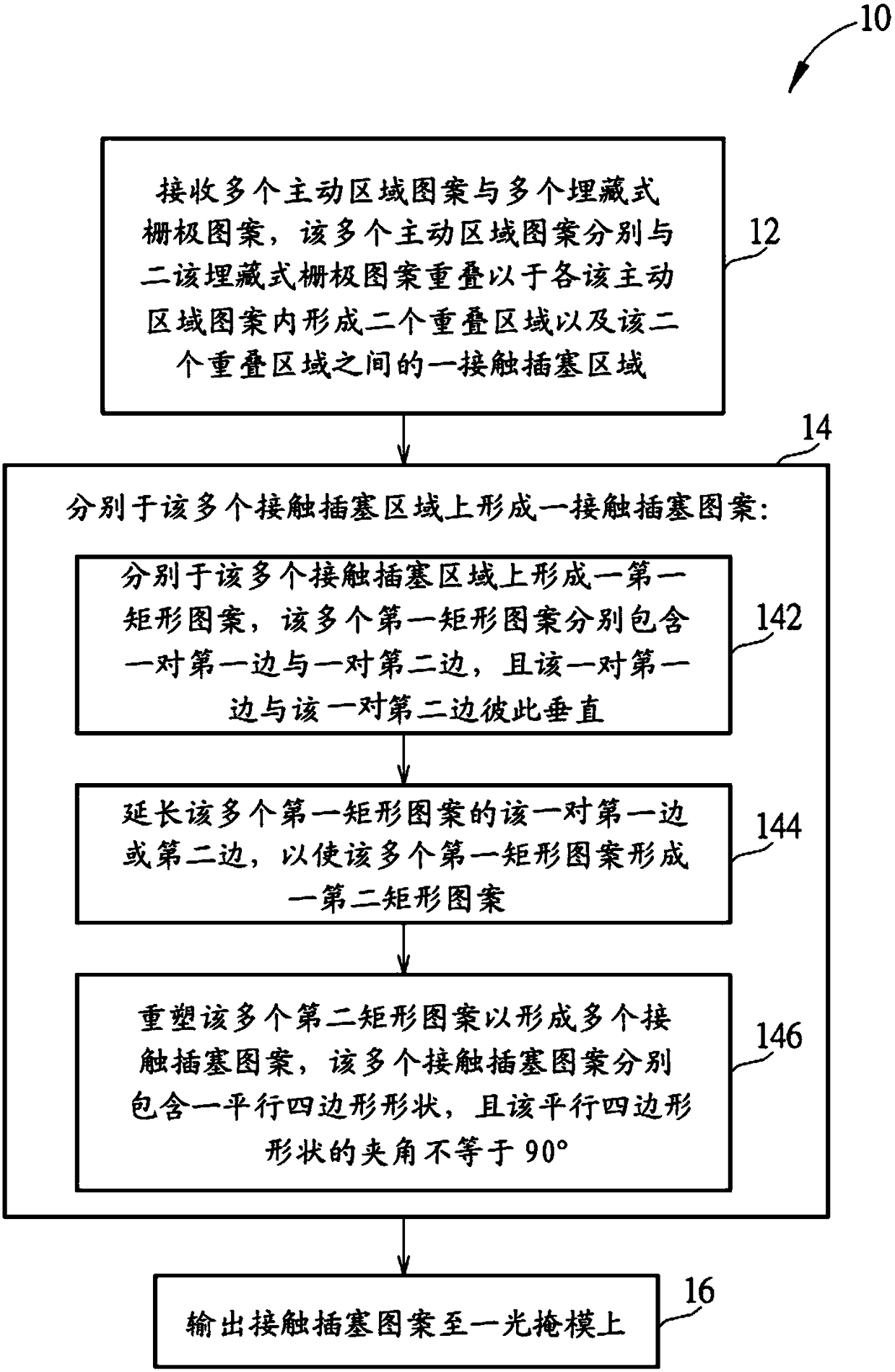
Manufacturing method for contact plug layout
A technology of contact plugs and manufacturing methods, which is applied in the direction of instruments, electrical digital data processing, electrical components, etc., can solve problems such as manufacturing process yield and product problems, short circuits, etc., and achieve the effect of improving the production process yield
- Summary
- Abstract
- Description
- Claims
- Application Information
AI Technical Summary
Problems solved by technology
Method used
Image

Examples
Embodiment Construction
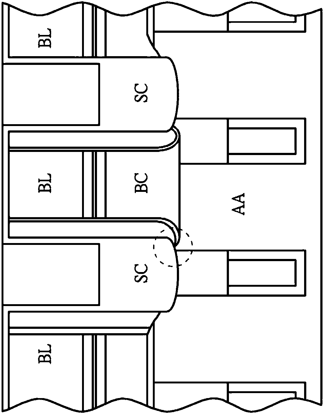
[0058] Those familiar with this technology should understand that the following provides a number of different embodiments to disclose different features of the present invention, but not limited thereto. In addition, the drawings disclosed below are simplified to express the features of the present invention more clearly, so the drawings disclosed below do not show all the elements of a specified element (or device). In addition, the drawings disclosed below are idealized schematic diagrams according to the present invention, so variations from these schematic diagrams, such as differences due to manufacturing techniques and / or tolerances, are expected. Therefore, the disclosure of the present invention should not be limited to the specific shapes disclosed in the accompanying drawings, but should also include deviations in shapes caused by manufacturing techniques.
[0059] In addition, those familiar with the technology should understand that in the following descriptions, ...
PUM
 Abstract
Description
Claims
Application Information
 - Generate Ideas
- Intellectual Property
- Life Sciences
- Materials
- Tech Scout
- Unparalleled Data Quality
- Higher Quality Content
- 60% Fewer Hallucinations
Browse by: Latest US Patents, China's latest patents, Technical Efficacy Thesaurus, Application Domain, Technology Topic, Popular Technical Reports.
© 2025 PatSnap. All rights reserved.Legal|Privacy policy|Modern Slavery Act Transparency Statement|Sitemap|About US| Contact US: help@patsnap.com