Al<2>O<3>/(La<2>O<3><x>(Al<2>O<3><1-x>/Al<2>O<3> structure-based nonvolatile storage device and preparation method thereof

A non-volatile storage and device technology, applied in the field of microelectronic materials, can solve problems such as increased leakage current, failure to act as an insulating medium, and poor data retention performance

Inactive Publication Date: 2018-08-31
ANYANG NORMAL UNIV
View PDF0 Cites 0 Cited by
  • Summary
  • Abstract
  • Description
  • Claims
  • Application Information

AI Technical Summary

Problems solved by technology

However, nitrides (Si 3 N 4 ) as a non-volatile memory device prepared as a storage layer has poor data retention performance, while the traditional SiO 2 The thickness of the tunneling layer and barrier layer is getting thinner and thinner, and the leakage current increases, which makes the tunneling layer and barrier layer unable to play the role of insulating medium.

Method used


Image

  • Al&lt;2&gt;O&lt;3&gt;/(La&lt;2&gt;O&lt;3&gt;&lt;x&gt;(Al&lt;2&gt;O&lt;3&gt;&lt;1-x&gt;/Al&lt;2&gt;O&lt;3&gt; structure-based nonvolatile storage device and preparation method thereof
  • Al&lt;2&gt;O&lt;3&gt;/(La&lt;2&gt;O&lt;3&gt;&lt;x&gt;(Al&lt;2&gt;O&lt;3&gt;&lt;1-x&gt;/Al&lt;2&gt;O&lt;3&gt; structure-based nonvolatile storage device and preparation method thereof
  • Al&lt;2&gt;O&lt;3&gt;/(La&lt;2&gt;O&lt;3&gt;&lt;x&gt;(Al&lt;2&gt;O&lt;3&gt;&lt;1-x&gt;/Al&lt;2&gt;O&lt;3&gt; structure-based nonvolatile storage device and preparation method thereof

Examples


Embodiment 1

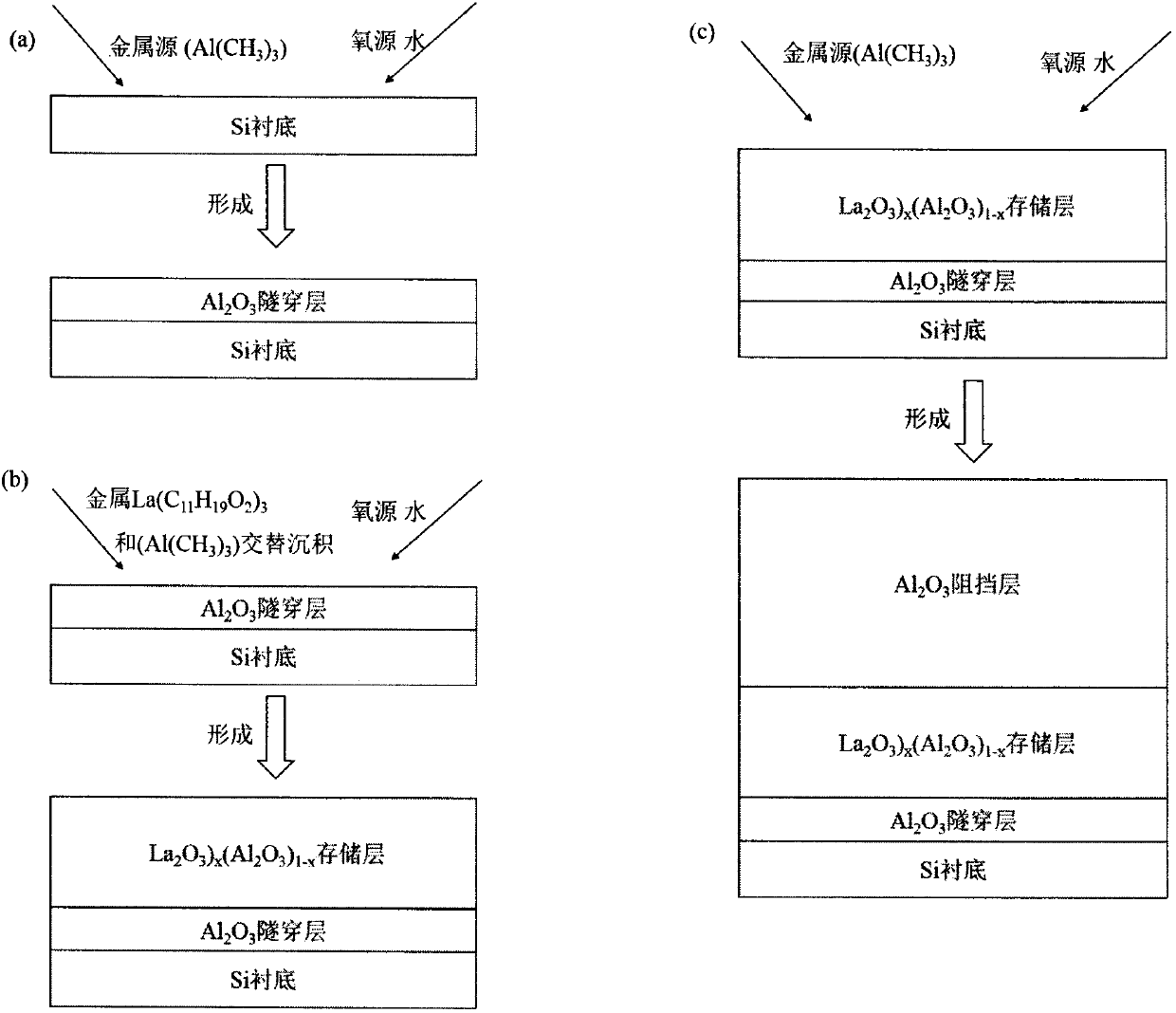
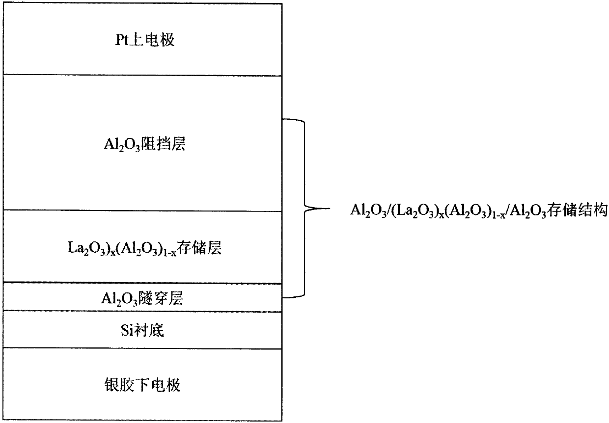
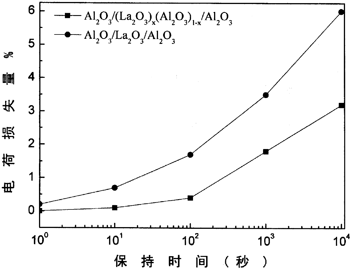
[0016] Example 1: with Al 2 o 3 / (La 2 o 3 ) x (Al 2 o 3 ) 1-x / Al 2 o 3 The preparation process of the non-volatile memory device of the memory structure is as follows:

[0017] a) Put the Si substrate into an appropriate amount of acetone, ultrasonically clean it for 3 minutes, and then ultrasonically clean it with deionized water for 3 minutes to remove residual impurities on the surface of the Si substrate. Then soak the substrate in 10% dilute hydrofluoric acid solution for 1 minute to remove oxides on the surface of the Si substrate, then use deionized water to ultrasonically clean it for 1 minute, dry it with high-purity nitrogen, and put it into the atomic layer chemistry In the vapor deposition chamber for thin film deposition;

[0018] b) A layer of Al is grown on the surface of the Si substrate by using the atomic layer chemical vapor deposition system 2 o 3 As the tunneling layer, trimethylaluminum Al(CH 3 ) 3 As the metal source, water is used as the...

Embodiment 2

[0022] Example 2: with Al 2 o 3 / La 2 o 3 / Al 2 o 3 The preparation process of the non-volatile memory device of the memory structure is as follows:

[0023] a) Put the Si substrate into an appropriate amount of acetone, ultrasonically clean it for 3 minutes, and then ultrasonically clean it with deionized water for 3 minutes to remove residual impurities on the surface of the Si substrate. Then soak the substrate in 10% dilute hydrofluoric acid solution for 1 minute to remove oxides on the surface of the Si substrate, then use deionized water to ultrasonically clean it for 1 minute, dry it with high-purity nitrogen, and put it into the atomic layer chemistry In the vapor deposition chamber for thin film deposition;

[0024] b) A layer of Al is grown on the surface of the Si substrate by using the atomic layer chemical vapor deposition system 2 o 3 As the tunneling layer, trimethylaluminum Al(CH 3 ) 3 As the metal source, water is used as the oxygen source, the numbe...


PUM


Abstract

The invention discloses an Al<2>O<3> / (La<2>O<3><x>(Al<2>O<3><1-x> / Al<2>O<3> structure-based nonvolatile storage device and a preparation method thereof. The Al<2>O<3> / (La<2>O<3><x>(Al<2>O<3><1-x> / Al<2>O<3> structure is grown on the surface of a Si substrate in sequence by adopting an atomic layer chemical vapor deposition method, wherein Al<2>O<3> close to the Si substrate is a tunneling layer; (La<2>O<3><x>(Al<2>O<3><1-x> is a storage layer; and Al<2>O<3> close to a metal electrode is a blocking layer. The obtained nonvolatile storage device is high in performance and simple in operation, andlarge-scale preparation can be realized.

Description

technical field [0001] The invention belongs to the field of microelectronic materials, and relates to a 2 o 3 / (La 2 o 3 ) x (Al 2 o 3 ) 1-x / Al 2 o 3 A nonvolatile memory device with a memory structure and a preparation method thereof. Background technique [0002] At present, the development of integrated circuits basically follows Moore's Law proposed by Gordon E. Moore in 1964, that is, the integration of integrated circuits doubles every 12 to 18 months, and the feature size shrinks. times. However, with the gradual reduction of device feature size, traditional floating gate non-volatile memory devices encounter material and technical bottlenecks, mainly due to the continuous reduction in the size of the tunneling layer, serious charge loss, and increased power consumption. . To solve this difficult problem, polysilicon-oxide-nitride-oxide-silicon (SONOS) type semiconductor memory devices have been extensively studied. However, nitrides (Si 3 N 4 ) as a...

Claims


Application Information

Patent Timeline
IPC IPC(8): H01L21/28H01L21/336H01L29/792C23C14/16C23C14/35C23C16/40C23C16/455
CPCH01L29/66833C23C14/165C23C14/35C23C16/403C23C16/409C23C16/45525H01L29/40117H01L29/792
Inventor 李荣汤振杰
Owner ANYANG NORMAL UNIV
Why Eureka
Try Eureka