Formation method of semiconductor structure

A technology of semiconductor and dummy gate structure, applied in semiconductor/solid-state device manufacturing, electrical components, circuits, etc., can solve problems such as adverse effects of semiconductor devices

Active Publication Date: 2020-05-08
SEMICON MFG INT (SHANGHAI) CORP +1
View PDF3 Cites 0 Cited by
  • Summary
  • Abstract
  • Description
  • Claims
  • Application Information

AI Technical Summary

Problems solved by technology

[0006] However, with the wide application of high-k dielectric materials, the adverse effects of high-k dielectric materials on semiconductor devices are becoming more and more serious

Method used


Image

  • Formation method of semiconductor structure
  • Formation method of semiconductor structure
  • Formation method of semiconductor structure

Examples


Embodiment Construction

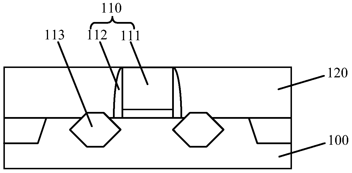
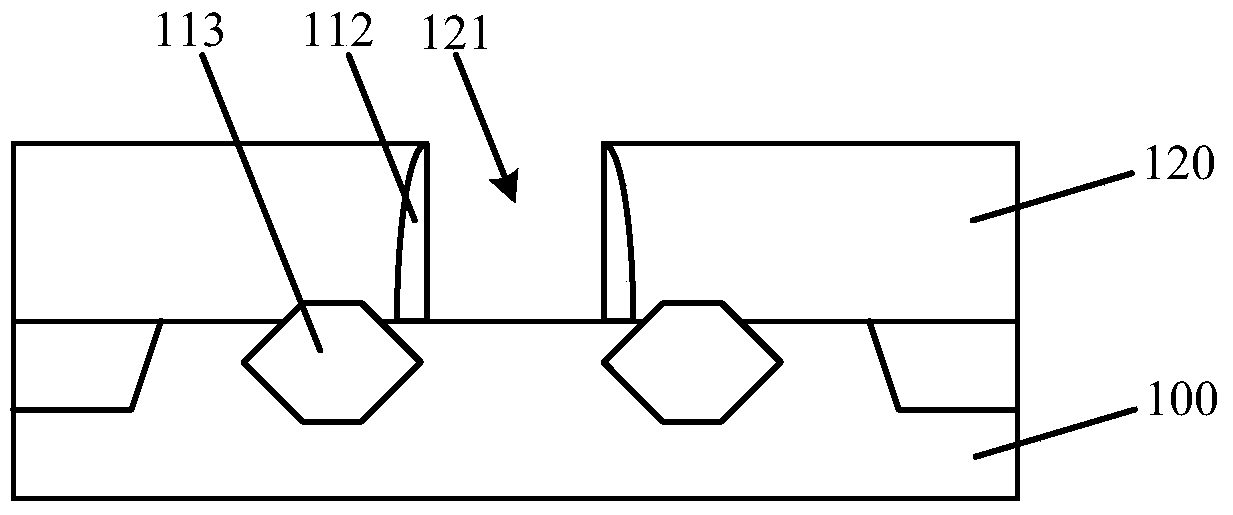
[0033] As mentioned in the background, with the wide application of high-k dielectric materials, the disadvantages of high-k dielectric materials have more and more serious adverse effects on semiconductor devices.

[0034] After research, it is found that the atoms in the high-k dielectric material will be polarized under the action of an alternating electric field, and will return to an electrical equilibrium state through a relaxation process, that is, the phenomenon of relaxation (Dielectric Relaxation, DR for short). During the relaxation process, the polarized atoms in the high-k dielectric material need a certain relaxation time to return to an electrical equilibrium state, and during the relaxation process, a relaxation current is generated in the high-k dielectric material, resulting in energy loss. Specifically, the polarization intensity in the high-k dielectric material has a phase angle lagging behind the alternating electric field, and the energy loss caused by t...


PUM


Abstract

The invention provides a method for forming a semiconductor structure. The method comprises a step of providing a substrate, a step of forming an interface layer at the surface of the substrate, a step of forming a high k dielectric layer at the surface of the interface layer, and a step of carrying out first annealing process which is used for doping optimization ions in the high k dielectric layer, wherein the optimization ions are used for filling the defects in the high k dielectric layer. The performance of the formed semiconductor structure is improved.

Description

technical field [0001] The invention relates to the technical field of semiconductor manufacturing, in particular to a method for forming a semiconductor structure. Background technique [0002] With the rapid development of integrated circuit manufacturing technology, the size of semiconductor devices in integrated circuits, especially MOS (Metal Oxide Semiconductor, metal-oxide-semiconductor) devices, is continuously reduced to meet the miniaturization and development of integrated circuits. Integration requirements, and transistor devices are one of the important components of MOS devices. [0003] For semiconductor devices, as the size of semiconductor devices continues to shrink, the gate dielectric layer formed of silicon oxide or silicon oxynitride material in the prior art cannot meet the performance requirements of semiconductor devices. In particular, transistors formed with silicon oxide or silicon oxynitride as the gate dielectric layer are prone to a series of ...

Claims


Application Information

Patent Timeline
Patent Type & Authority Patents(China)
IPC IPC(8): H01L21/3115H01L21/316
Inventor 李勇
Owner SEMICON MFG INT (SHANGHAI) CORP
Why Eureka
Try Eureka