Sandwich-structure thin film, preparation method and application thereof
A sandwich and thin-film technology, which is applied in vacuum evaporation plating, coating, ohmic resistance heating, etc., can solve the problems of low performance of sandwich-structured thin films, and achieve the effects of rapid response, excellent photoelectric performance and high efficiency
- Summary
- Abstract
- Description
- Claims
- Application Information
AI Technical Summary
Problems solved by technology
Method used
Image
Examples
Embodiment 1
[0062] A sandwich structure film with the structure of AZO(58nm) / Au(10nm) / AZO(62nm) / mica was prepared.
[0063] A 6 μm single-crystal flexible high-temperature-resistant mica substrate was obtained by mechanical stripping. The mica substrate was cleaned with nitrogen gas, coated with silver glue on the back of the mica, and the mica sheet was fixed on the substrate holder and installed in the cavity. The 99.9999wt% Au target and the 99.99wt% AZO target were fixed on a rotatable target stage in the cavity of the pulsed laser deposition device.
[0064] Adjust the target-base distance (the distance between the target and the substrate) to 60mm, and use the mechanical pump and the molecular pump to pump the gas in the chamber successively, so that the vacuum degree of the back and the bottom reaches 1×10 -4 Pa, then heat the mica substrate to 200°C at a heating rate of 20°C / min, open the oxygen inlet valve to pass ultra-pure oxygen into the chamber, adjust the oxygen inlet microf...
Embodiment 2
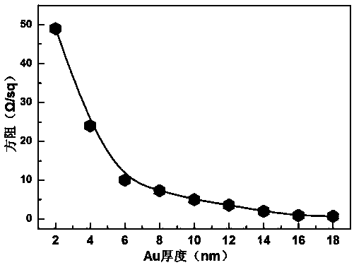
[0070] A sandwich structure film with the structure of AZO(58nm) / Au(2-18nm) / AZO(62nm) / mica was prepared.
[0071] According to the preparation process of Example 1, an AZO film with a thickness of 62nm, an Au film with a thickness of 2-18nm, and an AZO film with a thickness of 58nm are prepared successively on the mica substrate, wherein the thickness of the Au film is controlled to be 2, 4, 6, 8, 10, 12, 14, 16, 18nm, a series of sandwich structure films with different Au film thicknesses were prepared.
[0072] image 3 The square resistance of the sandwich structure film prepared for this example varies with the thickness of the interlayer Au film. like image 3 As shown, the average visible light transmittance of the square resistance of the sandwich structure film gradually decreases with the increase of the thickness of the Au film, and the square resistance decreases accordingly; when the thickness of the interlayer Au film increases from 2nm to 6nm, the sandwich stru...
Embodiment 3
[0074] Preparation of sandwich structure film with structure ZnO (58nm) / Ag(10nm) / ZnO (62nm) / mica
[0075] A 6 μm single-crystal flexible high-temperature-resistant mica substrate was obtained by mechanical stripping, and the mica substrate was cleaned with nitrogen; the Ag target and the ZnO target were fixed in the magnetron sputtering chamber, and the mica substrate was placed in the magnetron sputtering chamber Adjust the distance between the mica substrate and the target to 50 mm on the rotating heating stage.
[0076] Vacuumize the magnetron sputtering chamber and fill it with argon gas to clean the target material. When the air pressure reaches 10Pa, turn the mica substrate to the corresponding position of the ZnO target material, turn on the radio frequency power supply, and sputter the ZnO target material onto the mica substrate Above, a lower ZnO thin film with a thickness of 62nm was prepared.
[0077] Adjust the intake and exhaust volume, when the vacuum reaches 3×...
PUM
| Property | Measurement | Unit |
|---|---|---|
| thickness | aaaaa | aaaaa |
| thickness | aaaaa | aaaaa |
| thickness | aaaaa | aaaaa |
Abstract
Description
Claims
Application Information
 - R&D
- Intellectual Property
- Life Sciences
- Materials
- Tech Scout
- Unparalleled Data Quality
- Higher Quality Content
- 60% Fewer Hallucinations
Browse by: Latest US Patents, China's latest patents, Technical Efficacy Thesaurus, Application Domain, Technology Topic, Popular Technical Reports.
© 2025 PatSnap. All rights reserved.Legal|Privacy policy|Modern Slavery Act Transparency Statement|Sitemap|About US| Contact US: help@patsnap.com


