Low-power resistive switching memory cell based on doped strontium titanate film and its preparation method and application
A technology of resistive switch and storage unit, applied in the field of information storage, can solve the problems of no major breakthrough in reducing power consumption, large set/reset voltage, small on/off current ratio, etc., so as to reduce power consumption and reduce set /Reset voltage, effect of increasing ON/OFF current ratio
- Summary
- Abstract
- Description
- Claims
- Application Information
AI Technical Summary
Problems solved by technology
Method used
Image
Examples
Embodiment 1
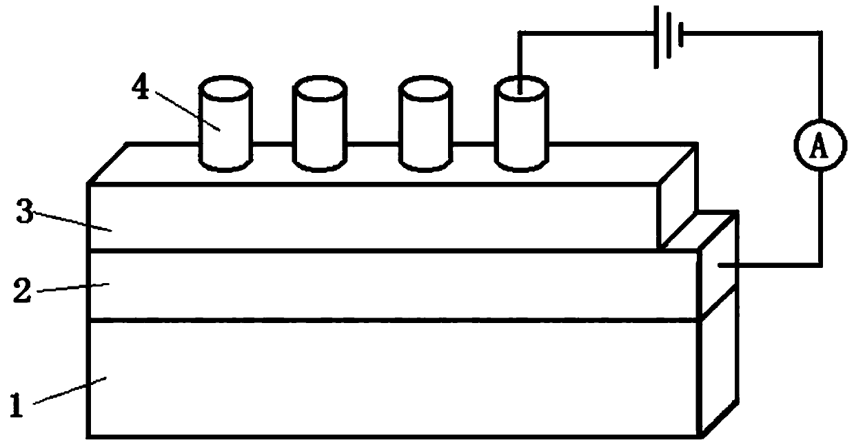
[0036] Embodiment 1, a method for preparing a low power consumption resistive switch memory cell based on a doped strontium titanate thin film, which includes the following steps:
[0037] Step 1: Select a conventional semiconductor Si single crystal substrate as the substrate, and prepare the lower electrode layer by DC magnetron sputtering in an argon atmosphere. The process conditions are: metal Pt is used as the sputtering target, and the sputtering gas is Argon gas, the sputtering pressure is 2.7Pa, the sputtering temperature is 350°C, the sputtering power is 35W, a bias voltage of -100V is applied, and the growth rate is 10-15nm / min;
[0038] In step 2, the substrate with the lower electrode layer is preheated at a temperature of 600° C., and then the Fe / strontium titanate thin film resistive layer is prepared on the lower electrode layer by radio frequency magnetron sputtering. The process conditions are: : Strontium titanate ceramic target with a purity of 99.9% and a ...
Embodiment 2
[0041] Embodiment 2, a method for preparing a low power consumption resistive switch memory cell based on a doped strontium titanate thin film, which includes the following steps:
[0042] Step 1: Select a conventional semiconductor Si single crystal substrate as the substrate, and prepare the lower electrode layer by DC magnetron sputtering in an argon atmosphere. The process conditions are: metal Pt is used as the sputtering target, and the sputtering gas is Argon gas, the sputtering pressure is 2Pa, the sputtering temperature is 300°C, the sputtering power is 25W, a bias voltage of -100V is applied, and the growth rate is 10-15nm / min;
[0043] In step 2, the substrate with the lower electrode layer is preheated at a temperature of 800° C., and then the Fe / strontium titanate thin film resistive layer is prepared on the lower electrode layer by radio frequency magnetron sputtering. The process conditions are: : Strontium titanate ceramic target with a purity of 99.9% and a Fe...
Embodiment 3
[0046] Embodiment 3, a method for preparing a low power consumption resistive switch memory cell based on a doped strontium titanate thin film, which includes the following steps:
[0047] Step 1: Select a conventional semiconductor Si single crystal substrate as the substrate, and prepare the lower electrode layer by DC magnetron sputtering in an argon atmosphere. The process conditions are: metal Pt is used as the sputtering target, and the sputtering gas is Argon gas, the sputtering pressure is 1Pa, the sputtering temperature is 400°C, the sputtering power is 45W, a bias voltage of -100V is applied, and the growth rate is 10-15nm / min;
[0048] In step 2, the substrate with the lower electrode layer is preheated at a temperature of 300° C., and then the Fe / strontium titanate thin film resistive layer is prepared on the lower electrode layer by radio frequency magnetron sputtering. The process conditions are: : Strontium titanate ceramic target with a purity of 99.9% and a Fe...
PUM
| Property | Measurement | Unit |
|---|---|---|
| thickness | aaaaa | aaaaa |
| thickness | aaaaa | aaaaa |
| thickness | aaaaa | aaaaa |
Abstract
Description
Claims
Application Information
 - R&D Engineer
- R&D Manager
- IP Professional
- Industry Leading Data Capabilities
- Powerful AI technology
- Patent DNA Extraction
Browse by: Latest US Patents, China's latest patents, Technical Efficacy Thesaurus, Application Domain, Technology Topic, Popular Technical Reports.
© 2024 PatSnap. All rights reserved.Legal|Privacy policy|Modern Slavery Act Transparency Statement|Sitemap|About US| Contact US: help@patsnap.com


