
Metal aluminum hole filling method

A technology of metal aluminum and process conditions, which is used in the manufacture of electrical components, circuits, semiconductor/solid-state devices, etc., and can solve the problems of large current load of metal layers, easy fusing of wires, cracks and voids in the film, etc.

Active Publication Date: 2020-06-09
SHANGHAI HUAHONG GRACE SEMICON MFG CORP
View PDF7 Cites 0 Cited by
  • Summary
  • Abstract
  • Description
  • Claims
  • Application Information

AI Technical Summary

Problems solved by technology

[0004] However, the main difficulty of metal aluminum hole filling is that the step coverage is not high. When the metal aluminum film crosses the steps on the substrate surface, it will deviate from the ideal situation. The film is thinner or cracks and cavities appear. The step coverage directly affects the metal wiring. Conductivity, which determines whether the circuit works efficiently
The current load of the metal layer on the top layer is large, and the heat dissipation of the wire is also large. If the step coverage is low, the current density passing through the wire will be high, and the wire will be easily fused; at the same time, the step coverage is low, the contact resistance will increase, and the delay of the circuit and power consumption will increase accordingly
Not only that, the thickness of the metal coverage on the steps is uneven, and voids caused by electromigration are prone to appear

Method used


Image

  • Metal aluminum hole filling method
  • Metal aluminum hole filling method
  • Metal aluminum hole filling method

Examples


Embodiment Construction

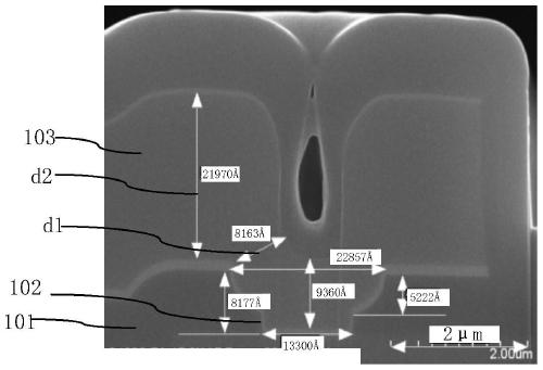
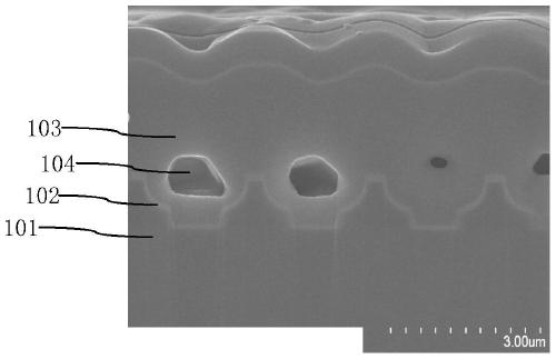
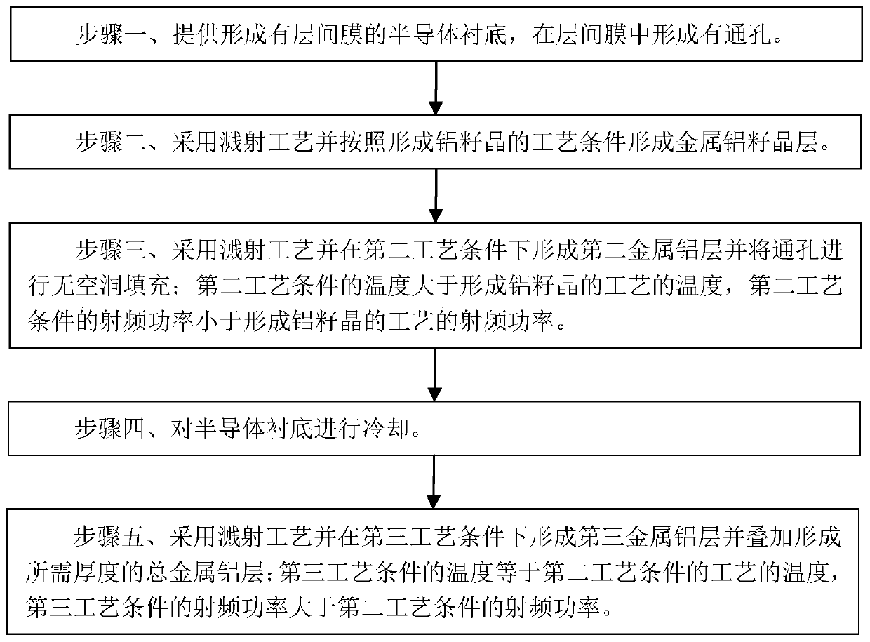
[0037] Such as image 3 Shown is the flow chart of the method for filling holes with metal aluminum in the embodiment of the present invention; as Figure 4 Shown is a photo of the appearance of the through hole 22 formed by the method of filling holes with metal aluminum according to the embodiment of the present invention. The method of filling holes with metal aluminum according to the embodiment of the present invention includes the following steps:

[0038] Step 1: providing a semiconductor substrate, an interlayer film 1 is formed on the semiconductor substrate, and a through hole 2 passing through the interlayer film 1 is formed in the interlayer film 1 .

[0039] In an embodiment of the present invention, the semiconductor substrate is a silicon substrate.

[0040] Preferably, the material of the interlayer film 1 is an oxide film.

[0041] The cross-sectional structure of the through hole 2 is divided into upper and lower parts, the side of the lower part is a verti...


PUM

PropertyMeasurementUnit
diameteraaaaaaaaaa
thicknessaaaaaaaaaa
widthaaaaaaaaaa

Abstract

The invention discloses a metal aluminum pore filling method. The metal aluminum pore filling method comprises the steps of providing a semiconductor substrate formed with an interlayer film and forming through holes in the interlayer film; adopting a sputtering technology to form a first metal aluminum seed crystal layer according to an aluminum seed crystal process condition; forming a second metal aluminum layer by adopting the sputtering technology in a second process condition, and performing no-void filling in the through holes, wherein the temperature in the second process condition ishigher than that in the aluminum seed crystal formation process, and the radio frequency power in the second process condition is lower than that in the aluminum seed crystal formation process; performing cooling on the semiconductor substrate; and forming a third metal aluminum layer by adopting the sputtering technology in a third process condition, and performing overlaying to form a total metal aluminum layer with the needed thickness, wherein the temperature in the third process condition is equal to that in the second process condition, and the radio frequency power in the third processcondition is higher than that in the second process condition. By virtue of the metal aluminum pore filling method, metal aluminum stage coverage rate is improved and the electrical performance and reliability of metal aluminum are improved.

Description

technical field [0001] The invention relates to a method for manufacturing a semiconductor integrated circuit, in particular to a method for filling holes with metal aluminum. Background technique [0002] In power discrete devices and power integrated circuits, usually power devices need to pass a large current, so a thick aluminum process is required, and the metal aluminum hole filling process is widely used. [0003] Compared with tungsten plugs, metal aluminum deposited by physical vapor deposition (PVD) has low resistivity, small RC delay of the circuit, and the integration process of metal aluminum is simple and low cost. Metal aluminum can connect metal contacts and metal interconnections It is completed once, and does not require etching back or chemical mechanical polishing (CMP) process similar to the tungsten plug process, which saves equipment and resources. That is to say, when the tungsten plug process is used, metal tungsten needs to be formed in the through...

Claims


Application Information

Patent Timeline
Patent Type & Authority Patents(China)
IPC IPC(8): H01L21/768
CPCH01L21/76876H01L21/76882H01L21/76883
Inventor 王星杰沈今楷刘春玲季芝慧
Owner SHANGHAI HUAHONG GRACE SEMICON MFG CORP
Learn More