A chip with expandable memory

A technology for expanding memory and memory, which is applied in memory address/allocation/relocation, instruments, computers, etc. It can solve the problems of increasing the average hops of memory modules and reducing the speed of memory modules, etc., to achieve load balance, reduce delay, and reduce burden Effect

Active Publication Date: 2020-10-16
HUAWEI TECH CO LTD
View PDF7 Cites 0 Cited by
  • Summary
  • Abstract
  • Description
  • Claims
  • Application Information

AI Technical Summary

Problems solved by technology

If each memory module is directly connected to the processor, the bandwidth that each memory module can use is only 1 / N (assuming that there are N memory modules directly connected to the processor); if multiple memory modules are used as a set of memory modules , and is directly connected to the processor through a memory module in the memory module set. Each memory module set can use a larger bandwidth, but the average number of hops for the processor to access the memory module increases, thereby reducing the processor access to the memory module. speed

Method used


Image

  • A chip with expandable memory
  • A chip with expandable memory
  • A chip with expandable memory

Examples


Embodiment Construction

[0030] The following will clearly and completely describe the technical solutions in the embodiments of the present invention with reference to the drawings in the embodiments of the present invention. Obviously, the described embodiments are part of the embodiments of the present invention, not all of them.

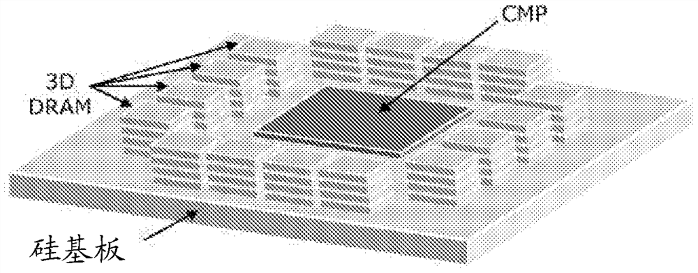
[0031] figure 1 A schematic structural diagram of an expandable memory chip 100 applicable to an embodiment of the present invention is shown. Such as figure 1 As shown, the chip 100 includes a multi-core processor chip (Chip of Multi Processor, CMP), multiple three-dimensional (Three-dimensional, 3D) dynamic random access memory (Dynamic Random Access Memory, DRAM) and the CMP and the multiple A DRAM integrated silicon substrate (silicon interposer), wherein the surface of the silicon substrate can be covered with a metal coating, and the DRAM and CMP can be inverted and integrated on the silicon substrate. A plurality of micro-bumps for communication are arranged bet...


PUM


Abstract

A chip (200) with expandable memory, the chip (200) comprising: a substrate (240), a processor (230) integrated on the substrate (240), a first memory module set (210) and a second memory module set (220); the processor (230) communicates with at least one memory module in the first memory module set (210) through a first communication interface (250), and the processor (230) communicates through a second The communication interface (260) communicates with at least one memory module in the second memory module set (220); the memory module in the first memory module set (210) communicates with the second memory module set (220) The memory modules in the device communicate through a substrate network, which is a communication network inside the substrate (240). The processor (230) can access the memory modules in the first memory module set (210) through the second memory module set (220), thereby reducing the time for the processor (230) to access the memory modules while ensuring high memory bandwidth Delay.

Description

technical field [0001] The invention relates to the field of integrated circuits, in particular to a chip with expandable memory. Background technique [0002] In-memory computing is a computing method that loads all data into the memory. By loading all the data into the memory, it avoids the import and export of data in the hard disk, thereby improving the processing speed of the chip. [0003] In-memory computing requires the capacity and bandwidth of larger memory, and therefore, requires a large number of memory modules connected to the processor. If each memory module is directly connected to the processor, the bandwidth that each memory module can use is only 1 / N (assuming that there are N memory modules directly connected to the processor); if multiple memory modules are used as a set of memory modules , and is directly connected to the processor through a memory module in the memory module set. Each memory module set can use a larger bandwidth, but the average numbe...

Claims


Application Information

Patent Timeline
Patent Type & Authority Patents(China)
IPC IPC(8): G06F12/02G06F13/14
CPCG06F2213/0038G06F13/4045G06F13/1668G06F15/7839H04L43/08G06F12/02G06F15/7807G06F13/14
Inventor 戴芬胡杏徐君王元钢
Owner HUAWEI TECH CO LTD
Why Eureka
Try Eureka