Over-temperature protection circuit, semiconductor device and fabrication method of semiconductor device

An over-temperature protection circuit and semiconductor technology, which is applied in the direction of semiconductor devices, semiconductor/solid-state device manufacturing, and electric solid-state devices, can solve the problems of poor temperature sensitivity of over-temperature protection circuits, and avoid process complexity and high cost. The effect of simplifying the design

Pending Publication Date: 2018-06-01
SHANGHAI NATLINEAR ELECTRONICS CO LTD
View PDF4 Cites 4 Cited by
  • Summary
  • Abstract
  • Description
  • Claims
  • Application Information

AI Technical Summary

Problems solved by technology

[0004] In view of the shortcomings of the prior art described above, the purpose of the present invention is to provide an over-temperature protection circuit, a semiconductor device and a preparation method thereof, which are used to solve the problem of poor temperature sensitivity of the over-temperature protection circuit in the prior art

Method used


Image

  • Over-temperature protection circuit, semiconductor device and fabrication method of semiconductor device
  • Over-temperature protection circuit, semiconductor device and fabrication method of semiconductor device
  • Over-temperature protection circuit, semiconductor device and fabrication method of semiconductor device

Examples


Embodiment 1

[0068] Such as figure 2 As shown, the present invention provides an over-temperature protection circuit 2, and the over-temperature protection circuit 2 includes:

[0069]A semiconductor device 21 and a control module 22 ; the semiconductor device 21 includes a MOS field effect transistor 211 and a temperature sampling tube 212 ; the control module 22 includes a current source 221 , a comparator 222 and a control signal generating unit 223 .

[0070] Such as figure 2 As shown, one end of the current source 221 is connected to the power supply voltage VDD, and the other end is grounded after passing through the temperature sampling tube 212 to provide a constant current source.

[0071] Specifically, in this embodiment, the temperature sampling tube 212 is a diode, the anode of the diode is connected to the input terminal of the comparator 222 (inverting input terminal in this embodiment), and the cathode is grounded to VSS. In practical applications, the temperature sampli...

Embodiment 2

[0087] Such as Figure 6 As shown, the present invention provides a method for preparing the semiconductor device 21, the specific steps are as follows:

[0088] Step S1 : providing a substrate 214 , and performing termination implantation on the substrate 214 to form a termination region 213 .

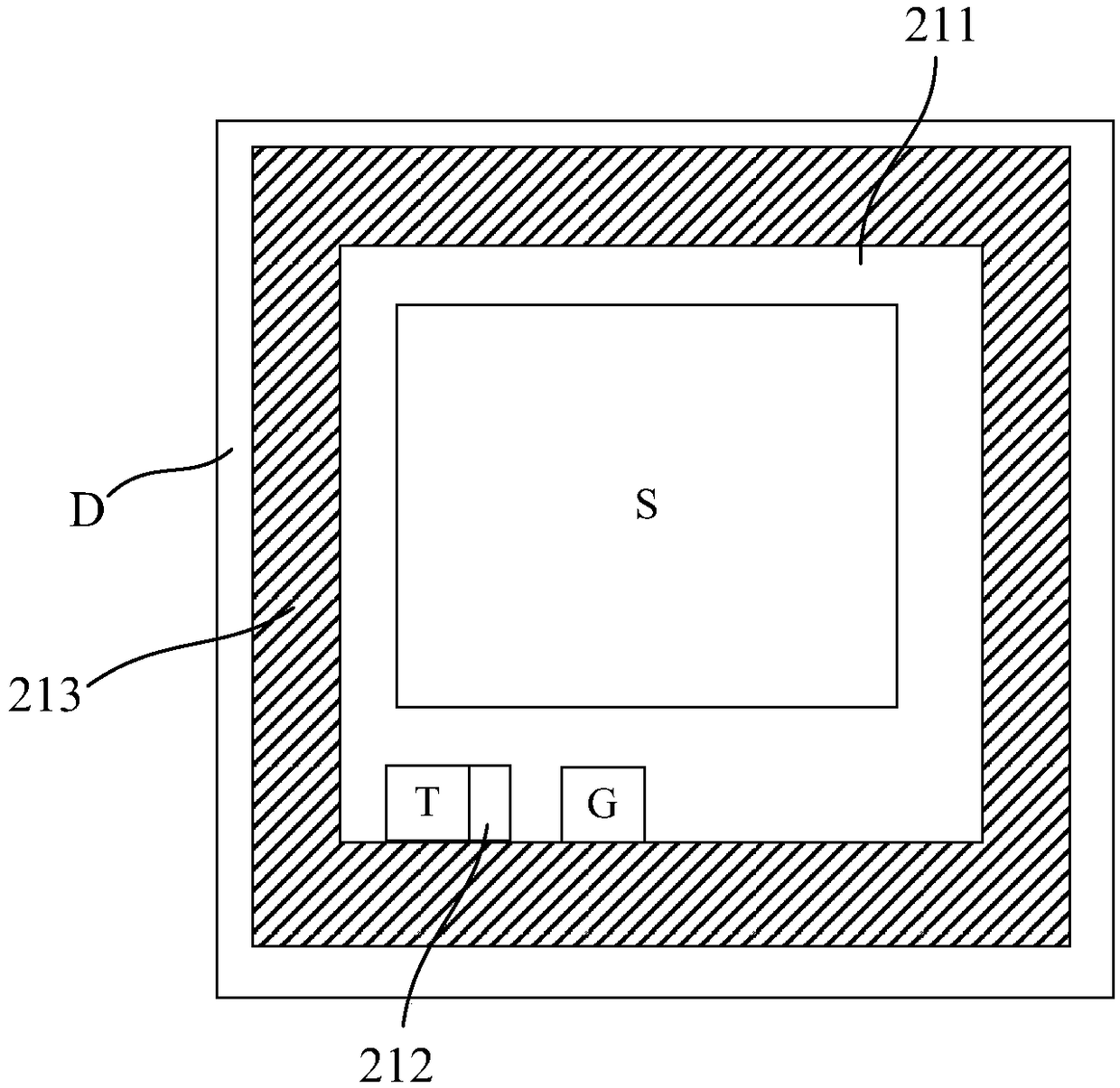
[0089] Specifically, such as Figure 6 As shown, in this embodiment, the conductivity type of the substrate 214 is N-type doping, an epitaxial layer 214a is formed on the substrate 214, and the conductivity type of the epitaxial layer 214a is N-type doping, and The doping concentration is smaller than the doping concentration of the substrate 214 . Perform oxidation treatment on the surface of the epitaxial layer 214a, then perform terminal photolithography, and form the terminal region 213 by ion implantation, as image 3 and Figure 6 As shown, the terminal area 213 is a ring structure.

[0090] Step S2: Form a field oxygen layer 215 on the surface of the epitaxial layer 214a s...


PUM


Abstract

The invention provides an over-temperature protection circuit, a semiconductor device and a fabrication method of the semiconductor device. The over-temperature protection circuit comprises a currentsource, a temperature sampling tube, a comparator, a control signal generation unit and an MOS field-effect transistor, wherein the current source is used for providing a constant-current source, thetemperature sampling tube is used for detecting a temperature, the comparator is used for generating a temperature detection signal according to the detected temperature, the control signal generationunit is used for generating a temperature control signal according to the temperature detection signal, and the MOS field-effect transistor is used for achieving over-temperature protection by switch-off or switch-on according to the temperature control signal. The real-time temperature can be timely and accurately acquired by a temperature sampling device, so that the over-temperature protectioncircuit effectively works, an error during the heat transferring process is not needed to be considered, and the design of the over-temperature protection circuit is simplified; and meanwhile, the semiconductor device and a control module are integrated in a package tube shell by a joint sealing mode to form the over-temperature protection circuit, chips based on different processed are organically combined, and process complexity and high cost brought by a single chip for achieving the same function are prevented.

Description

technical field [0001] The invention relates to the field of semiconductor manufacturing, in particular to an over-temperature protection circuit, a semiconductor device and a preparation method thereof. Background technique [0002] Such as figure 1 Shown is a schematic structural diagram of an existing high-power power management chip 1, wherein the integrated circuit 11 is set as a control circuit in one chip, including a control module 112; the power device 12 is set in another chip, including a power switch tube 121; Both are integrated in one package. The high-power power management chip generates a lot of heat. In order to better protect the chip from being burned by excessive heat during work, a built-in temperature sampling device 111 is usually built in to cooperate with the control module 112 to achieve over-temperature protection. The existing temperature sampling The device 111 is generally provided in the integrated circuit 11 . [0003] The integrated circu...

Claims


Application Information

Patent Timeline
Patent Type & Authority Applications(China)
IPC IPC(8): H01L27/02H01L21/8249H03K17/082H03K17/687
CPCH01L27/0259H01L27/0296H03K17/0822H03K17/687H01L21/8249H03K2017/0806
Inventor 何云王冬峰周尧刘桂芝
Owner SHANGHAI NATLINEAR ELECTRONICS CO LTD
Why Eureka
Try Eureka