Fin field effect transistor and formation method thereof

A fin field effect and transistor technology, which is applied in semiconductor devices, semiconductor/solid-state device manufacturing, electrical components, etc., can solve the problems that the performance of fin field effect transistors needs to be improved, achieve enhanced isolation performance, meet process design, improve The effect of electrical properties

Inactive Publication Date: 2018-05-22
SEMICON MFG INT (SHANGHAI) CORP +1
View PDF6 Cites 0 Cited by
  • Summary
  • Abstract
  • Description
  • Claims
  • Application Information

AI Technical Summary

Problems solved by technology

[0004] However, the performance of fin field effect transistors formed by existing technologies needs to be improved

Method used


Image

  • Fin field effect transistor and formation method thereof
  • Fin field effect transistor and formation method thereof
  • Fin field effect transistor and formation method thereof

Examples


Embodiment Construction

[0035] As mentioned in the background, the performance of the FinFETs formed in the prior art needs to be improved.

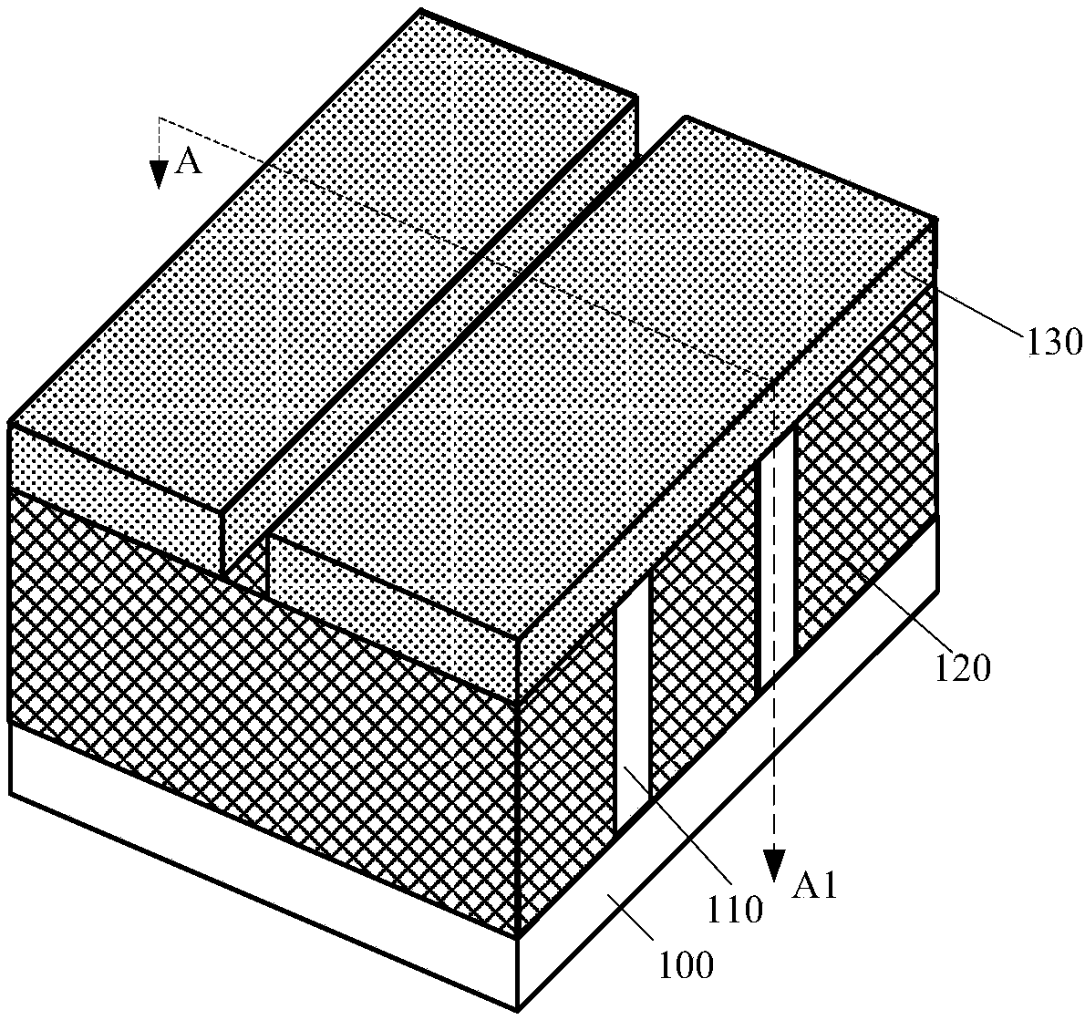
[0036] Figure 1 to Figure 4 It is a structural schematic diagram of the formation process of a fin field effect transistor.

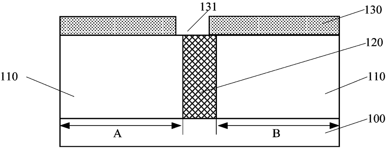
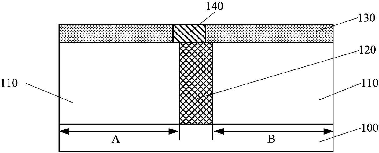
[0037] combined reference figure 1 with figure 2 , figure 2 for along figure 1 A schematic diagram obtained by cutting line A-A1 in the middle, a substrate 100 is provided, and the substrate 100 has a fin portion 110 on it, and the fin portion 110 includes a first region A and a second region B, and between the first region A and the second region B There is an isolation groove (not marked) between them; an isolation structure film 120 covering the sidewall of the fin portion 110 is formed on the substrate 100, and the isolation structure film 120 fills the isolation groove; formed on the isolation structure film 120 and on the fin portion 110 The patterned mask layer 130 has an opening 131 therein, and the opening 131 exposes p...


PUM


Abstract

The invention relates to a fin field effect transistor and a formation method thereof. The method includes the following steps that: a semiconductor substrate is provided, wherein the semiconductor substrate is provided with a fin portion; a sacrificial layer is formed on the semiconductor substrate and the fin portion, and the top surface of the sacrificial layer is higher than the top surface ofthe fin portion; a groove is formed in the sacrificial layer and the fin portion, and the groove penetrates the fin portion along a direction which is perpendicular to the extending direction of thefin portion and parallel to the surface of the semiconductor substrate; an isolation layer is formed in the groove, the top surface of the isolation layer is higher than the top surface of the fin portion; and after the isolation layer is formed, the sacrificial layer is removed. With the method adopted, the isolation layer higher than the top surfaces of a first fin portion and a second fin portion can fully cover the isolation layer lower than the top surfaces of the first fin portion and the second fin portion, and therefore, and therefore, the isolation performance of the isolation layer is enhanced, and process design requirements can be met.

Description

technical field [0001] The invention relates to the field of semiconductor manufacturing, in particular to a fin field effect transistor and a forming method thereof. Background technique [0002] MOS transistors are one of the most important components in modern integrated circuits. The basic structure of a MOS transistor includes: a semiconductor substrate; a gate structure located on the surface of the semiconductor substrate, a source region located in the semiconductor substrate on one side of the gate structure, and a drain region located in the semiconductor substrate on the other side of the gate structure. The working principle of the MOS transistor is: by applying a voltage to the gate structure, the current through the channel at the bottom of the gate structure is adjusted to generate a switching signal. [0003] With the development of semiconductor technology, the ability of the traditional planar MOS transistor to control the channel current becomes weaker, r...

Claims


Application Information

Patent Timeline
IPC IPC(8): H01L21/336H01L29/78
CPCH01L29/66795H01L29/785
Inventor 肖芳元王彦韩秋华蒋鑫张海洋
Owner SEMICON MFG INT (SHANGHAI) CORP
Why Eureka
Try Eureka