Substrate integrated spoof surface plasmon polariton waveguide
A technology of artificial surface plasmon and substrate integrated waveguide, which is applied in the direction of waveguide, waveguide-type devices, electrical components, etc., can solve the problems of difficult processing, large volume, high cost, etc., and achieve the reduction of electromagnetic wave radiation phenomenon, strong binding performance, The effect of artificial design convenience
- Summary
- Abstract
- Description
- Claims
- Application Information
AI Technical Summary
Problems solved by technology
Method used
Image
Examples
Embodiment 1
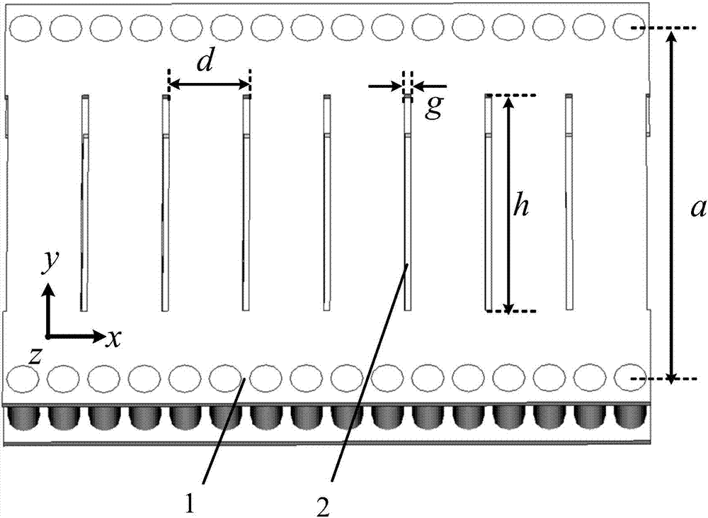
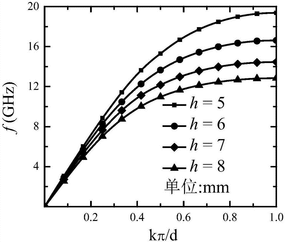
[0019] Integrate artificial surface plasmon waveguides for double-sided rectangular slotted substrates, such as figure 1 As shown, Embodiment 1 is provided with a substrate integrated waveguide 1 and a metal slot 2, the metal slot 2 is provided in the substrate integrated waveguide 1, the metal slot 2 is a periodic metal slot, and the metal slot 2 Distributed on one side of the substrate integrated waveguide 1 or distributed on both sides of the substrate integrated waveguide 1 in the manner of symmetry, anti-symmetry, offset symmetry, etc., it is used to transmit microwave and terahertz artificial For surface plasmon, the material of the dielectric substrate is Rogers RT5880, the dielectric constant is 2.2, the thickness is 0.508mm, and the transmission loss angle is 0.0009; the material of the metal film transmission line and the metal through hole is copper. The unit structure size of the waveguide is selected as a=12mm, d=2.5mm, and h is increased from 5mm to 8mm. The disp...
Embodiment 2
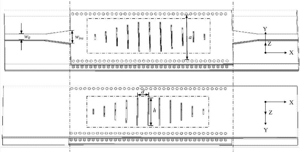
[0021] The bandpass filter designed for application example 1, such as image 3 shown. The filter is divided into three parts, the left and right ends are microstrip transmission lines, and the middle is a substrate-integrated artificial surface waveguide with double-sided rectangular metal slots. The filter has a symmetrical structure, and both ends are feeding terminals, w 0 =1.6mm, which guarantees the port impedance of 50Ω. The electromagnetic wave is converted from the microstrip line to the substrate-integrated waveguide by the tapered gradient transition structure, w tra =3.5mm, which realizes impedance matching with the substrate integrated waveguide. In order to achieve wave vector matching, the metal slot height is distributed with a gradient increase. Other main parameters are as follows: a=12mm, d=2.5mm, h=8mm. Depend on Figure 4 The simulation results show that the band-pass range of the filter is 8.5GHz to 12.3GHz, and it has relatively steep rising and fa...
PUM
| Property | Measurement | Unit |
|---|---|---|
| Thickness | aaaaa | aaaaa |
Abstract
Description
Claims
Application Information
 - Generate Ideas
- Intellectual Property
- Life Sciences
- Materials
- Tech Scout
- Unparalleled Data Quality
- Higher Quality Content
- 60% Fewer Hallucinations
Browse by: Latest US Patents, China's latest patents, Technical Efficacy Thesaurus, Application Domain, Technology Topic, Popular Technical Reports.
© 2025 PatSnap. All rights reserved.Legal|Privacy policy|Modern Slavery Act Transparency Statement|Sitemap|About US| Contact US: help@patsnap.com


