N-Ge-i-Ge-p-Si structural waveguide-type photoelectric detector based on LRC technology and manufacturing method

A photodetector, n-ge-i-ge-p-si technology, used in semiconductor devices, circuits, electrical components, etc., can solve the problems of poor thermal conductivity and mechanical properties, poor compatibility, limited application, etc. Low thermal budget, short process cycle time, and the effect of reducing dark current

Inactive Publication Date: 2018-03-30
TIBET UNIVERSITY FOR NATIONALITIES
View PDF3 Cites 4 Cited by
  • Summary
  • Abstract
  • Description
  • Claims
  • Application Information

AI Technical Summary

Problems solved by technology

However, its high price, poor thermal conductivity and mechanical properties, and poor compatibility with existing mature Si processes limit its application in Si-based optoelectronic integration technology.

Method used


Image

  • N-Ge-i-Ge-p-Si structural waveguide-type photoelectric detector based on LRC technology and manufacturing method
  • N-Ge-i-Ge-p-Si structural waveguide-type photoelectric detector based on LRC technology and manufacturing method
  • N-Ge-i-Ge-p-Si structural waveguide-type photoelectric detector based on LRC technology and manufacturing method

Examples


Embodiment 1

[0046] See figure 1 , figure 1 It is a schematic top view of an n-Ge-i-Ge-p-Si structure waveguide photodetector based on the LRC process provided by an embodiment of the present invention. The photodetector includes an SOI substrate and a waveguide, a coupling structure and a device part arranged on the top Si layer of the SOI substrate. The device part is finally formed into a photoelectric device through a semiconductor process to form a waveguide type photodetector.

[0047] It should be noted that the epitaxial Ge semiconductor material on the Si substrate is not only fully compatible with the existing Si process, but also has good response characteristics to the C-band (1528-1560 nm) optical signal in optical communication, and is applied to Si-based The photoelectric integration technology has great potential. At the same time, if the Ge PiN photodetector has a waveguide structure, because the light transmission and absorption are along the waveguide direction, and the car...

Embodiment 2

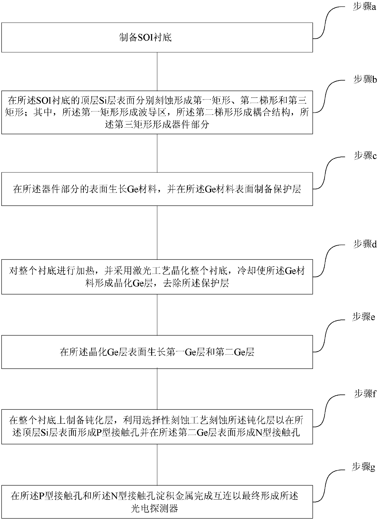
[0080] See also Figure 3a-Figure 3k , Figure 3a-Figure 3k It is a schematic diagram of a manufacturing method of an n-Ge-i-Ge-p-Si structure waveguide photodetector based on the LRC process provided by an embodiment of the present invention. In this embodiment, on the basis of the foregoing embodiment, the preparation method of the n-Ge-i-Ge-p-Si structure waveguide photodetector based on the LRC process of the present invention is described in detail as follows:

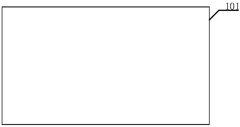
[0081] S101. The substrate is selected. Such as Figure 3a As shown, a single crystal silicon (Si) substrate sheet (001) is selected as the initial material 101;

[0082] S102, SOI substrate preparation. Such as Figure 3b As shown, choose O + The dose is 1.8×10 18 cm -2 Perform oxygen injection isolation, and then high-temperature annealing to form 1μm thick SiO 2 The SOI substrate with layer 102 and Si layer 103 of 1.5 μm thick.

[0083] S103. Preparation of waveguide and coupling region. Selectively etch to form a ...


PUM


Abstract

The invention relates to an n-Ge-i-Ge-p-Si structural waveguide-type photoelectric detector based on an LRC technology and a manufacturing method. The method comprises the following steps of manufacturing a SOI substrate; etching and forming a waveguide area, a coupling structure and a device poriton on a top layer Si layer surface respectively; growing a Ge material on a surface of the device portion and manufacturing a protection layer; heating a whole substrate, using a laser technology to crystallize the whole substrate, cooling and making the Ge material form a crystallization Ge layer, and removing the protection layer; growing a first Ge layer and a second Ge layer on a crystallization Ge layer surface; manufacturing a passivation layer on the whole substrate, using a selective etching technology to etch the passivation layer so as to form a P-type contact hole on the top layer Si layer surface and an N-type contact hole on a second Ge layer surface; and depositing metal in theP-type and N-type contact holes and completing interconnection so as to finally form the photoelectric detector. In the invention, by using the photoelectric detector, dark currents can be reduced, aconflict of a high speed response and quantum efficiency in a vertical light-entering-type optical detector is overcome, simultaneously a high speed and high quantum efficiency are guaranteed.

Description

Technical field [0001] The invention belongs to the technical field of integrated circuits, and specifically relates to an n-Ge-i-Ge-p-Si structure waveguide photodetector based on LRC technology and a preparation method thereof. Background technique [0002] As the minimum feature size continues to decrease in accordance with Moore's Law, the electrical interconnection of integrated circuits has brought a series of problems such as transmission delay and bandwidth density. Therefore, optical interconnection has become a better choice for modern integrated circuits, where photodetectors convert optical signals into electrical signals are one of the key components of optoelectronic integration. With the development of optical communication technology, photodetectors with high responsivity, high quantum efficiency, low dark current and high response frequency bandwidth have been realized. [0003] At present, semiconductor detectors mainly use III-V semiconductor materials such as I...

Claims


Application Information

Patent Timeline
Patent Type & Authority Applications(China)
IPC IPC(8): H01L31/028H01L31/0352H01L31/101H01L31/18
CPCH01L31/0284H01L31/035209H01L31/101H01L31/1812Y02P70/50
Inventor 乔丽萍
Owner TIBET UNIVERSITY FOR NATIONALITIES
Why Eureka
Try Eureka