Nitride semiconductor structure and semiconductor light-emitting element

A nitride semiconductor, semiconductor technology, applied in the direction of semiconductor devices, electrical components, circuits, etc., can solve the problems of loss of carriers, affecting the luminous efficiency of light-emitting diodes, and reducing the luminous efficiency of light-emitting diodes.

Inactive Publication Date: 2018-03-20
GENESIS PHOTONICS INC
View PDF8 Cites 0 Cited by
  • Summary
  • Abstract
  • Description
  • Claims
  • Application Information

AI Technical Summary

Problems solved by technology

[0007] The existing electron blocking layer is formed of a P-type AlGaN layer with a relatively large energy gap, thereby preventing electrons injected from the N-type semiconductor layer from overflowing into the P-type semiconductor layer, so that the electrons can be effectively confined in the quantum well layer , to improve the internal quantum efficiency of light-emitting diodes; however, although the electron blocking layer of P-AlGaN has a relatively large energy gap to prevent electron overflow, it also leads to a relatively poor effect of hole injection into the light-emitting layer; moreover , because the multiple quantum well structure is generally formed by the quantum well layer of InGaN and the quantum barrier layer of GaN, but in essence, the electron blocking layer of P-AlGaN and the quantum barrier layer of GaN have a very high lattice mismatch , so that the InGaN quantum well layer will be seriously affected by compressive stress due to lattice mismatch, and this compressive stress changes the energy band structure of each quantum well layer, so that the electrons and holes in the quantum well layer Spatially separated from each other, resulting in a reduction in the luminous efficiency of the light-emitting diode; moreover, the above-mentioned compressive stress will also deteriorate the interface characteristics between the adjacent GaN quantum barrier layer and the InGaN quantum well layer, thereby losing carriers at the interface, and also Affects the luminous efficiency of light-emitting diodes

Method used


Image

  • Nitride semiconductor structure and semiconductor light-emitting element
  • Nitride semiconductor structure and semiconductor light-emitting element

Examples


Embodiment Construction

[0035] The purpose of the present invention and its structural design and functional advantages will be described according to the following drawings and preferred embodiments, so as to have a more in-depth and specific understanding of the present invention.

[0036] First, in the description of the following embodiments, it should be understood that when it is indicated that a layer (or film) or a structure is disposed "on" or "under" another substrate, another layer (or film), or another structure, It can be "directly" located on other substrates, layers (or films), or another structure, or can be configured "indirectly" with more than one intermediate layer between them. The location of each layer can be described with reference to the drawings.

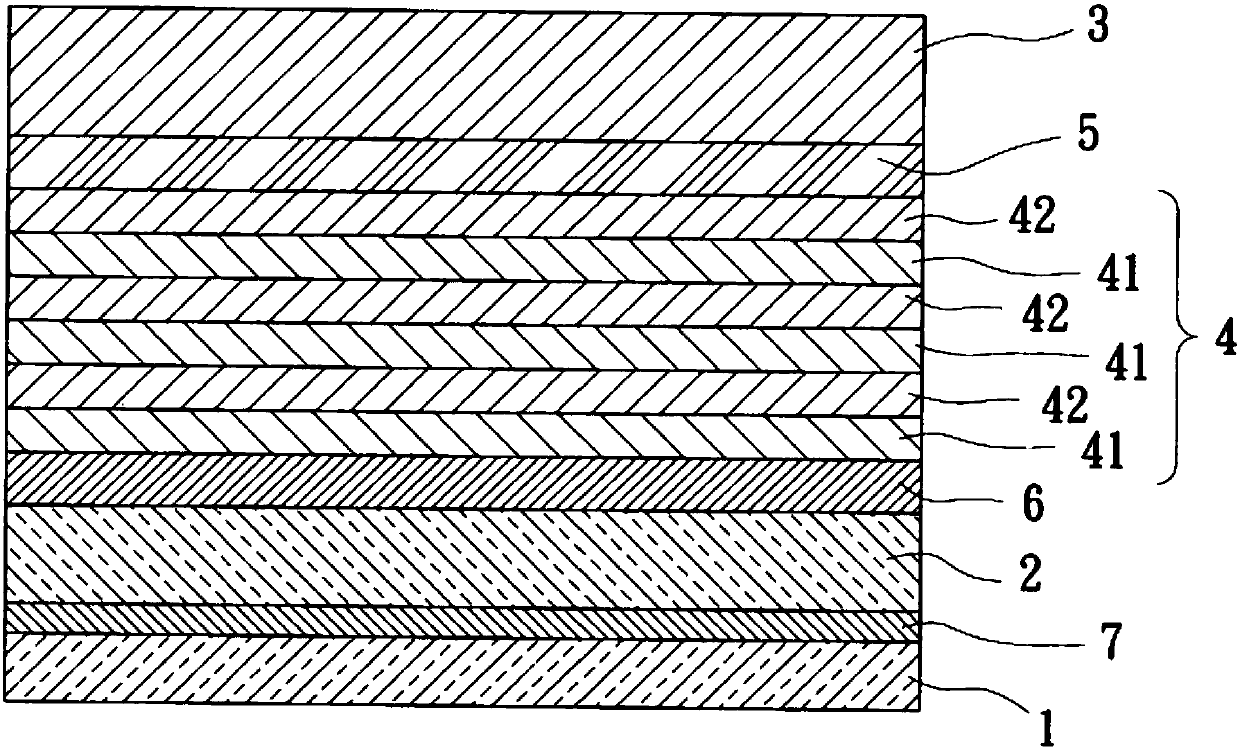
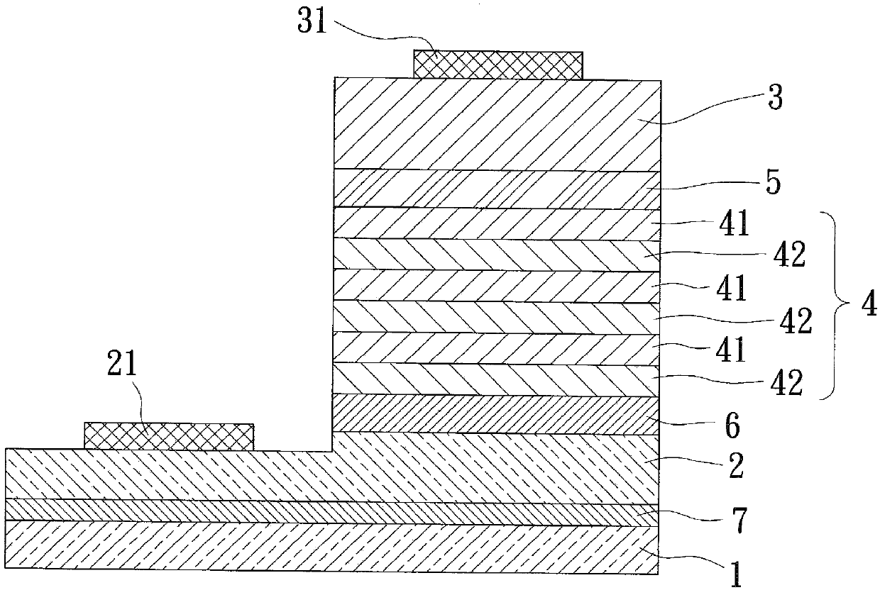
[0037] see figure 1 As shown, it is a schematic cross-sectional view of a nitride semiconductor structure provided by a preferred embodiment of the present invention, which includes an N-type semiconductor layer 2 and a P-type s...


PUM


Abstract

The invention relates to a nitride semiconductor structure and a semiconductor light-emitting element. The nitride semiconductor structure is mainly as follows: a light-emitting layer is arranged between an N-type semiconductor layer and a P-type semiconductor layer, wherein a quaternary carrier active layer is arranged between the light-emitting layer and the P-type semiconductor layer; and the quaternary carrier active layer is Al<x>In<y>Ga<1-x-y>N, wherein x and y are numerical values meeting the conditions as follows: x is smaller than 1 and greater than 0, y is smaller than 1 and greaterthan 0 and x+y is smaller than 1 and greater than 0. The semiconductor light-emitting element comprises the nitride semiconductor structure on a substrate, an N-type electrode and a P-type electrode,wherein the N-type electrode is matched with the P-type electrode to provide electric energy. Therefore, compared with a known P-AlGaN electron blocking layer, the nitride semiconductor structure andthe semiconductor light-emitting element have the advantages that the effect of electron holes entering a multi-quantum well structure can be improved, and meanwhile, the target of inhibiting electrons from escaping into the P-type semiconductor layer is achieved, so that the combination probability of the electrons and the electron holes is improved and the light-emitting efficiency is further improved.

Description

[0001] related divisional application [0002] This application is a divisional application of a patent with an application date of January 25, 2013, an application number of 201310028759.6, and an invention title of "Nitride Semiconductor Structure and Semiconductor Light-Emitting Element". technical field [0003] The present invention relates to a nitride semiconductor structure and a semiconductor light-emitting element, in particular to an aluminum indium gallium nitride Al x In y Ga 1-x-y The invention relates to a nitride semiconductor structure of a quaternary carrier active layer of N and a semiconductor light-emitting element, belonging to the technical field of semiconductors. Background technique [0004] In recent years, due to the advancement of epitaxy and process technology, light-emitting diodes have become one of the most promising solid-state lighting sources; among them, light-emitting diodes with gallium nitride (GaN) as the main manufacturing materia...

Claims


Application Information

Patent Timeline
Patent Type & Authority Applications(China)
IPC IPC(8): H01L33/06H01L33/12H01L33/14H01L33/32
CPCH01L33/06H01L33/12H01L33/14H01L33/145H01L33/32H01L33/325
Inventor 王信介李玉柱吴俊德林京亮李允立
Owner GENESIS PHOTONICS INC
Why Eureka
Try Eureka