
High voltage semiconductor device

A semiconductor and high-voltage technology, applied in the direction of semiconductor devices, semiconductor/solid-state device manufacturing, electrical components, etc., can solve the problems of breakdown voltage drop and leakage probability increase, so as to reduce the breakdown voltage drop, reduce the leakage probability, Effect of Preventing Leakage Current

Active Publication Date: 2020-05-26
NUVOTON
View PDF5 Cites 0 Cited by
  • Summary
  • Abstract
  • Description
  • Claims
  • Application Information

AI Technical Summary

Problems solved by technology

[0003] In traditional high-voltage semiconductor devices, the isolation structure (such as a field oxide layer) is directly exposed under the protective layer or molding compound, and cracks may be generated during the formation of the above materials, allowing mobile charges to penetrate into the field On the oxide layer, the breakdown voltage decreases and the probability of leakage increases

Method used


Image

  • High voltage semiconductor device
  • High voltage semiconductor device
  • High voltage semiconductor device

Examples


Embodiment Construction

[0041] The high-voltage semiconductor device and its manufacturing method of the present invention will be described in detail below. It should be appreciated that the following description provides many different embodiments or examples for implementing different aspects of the invention. The specific components and arrangements described below are intended to briefly describe the present invention. Of course, these are just examples and not intended to limit the scope of the present invention. Furthermore, repeated reference numerals or designations may be used in different embodiments. These repetitions are only for the purpose of simply and clearly describing the present invention, and do not represent any relationship between the different embodiments and / or structures discussed. Furthermore, for example, when it is mentioned that a first material layer is located on or over a second material layer, the situation that the first material layer is in direct contact with t...


PUM

PropertyMeasurementUnit
breakdown voltageaaaaaaaaaa

Abstract

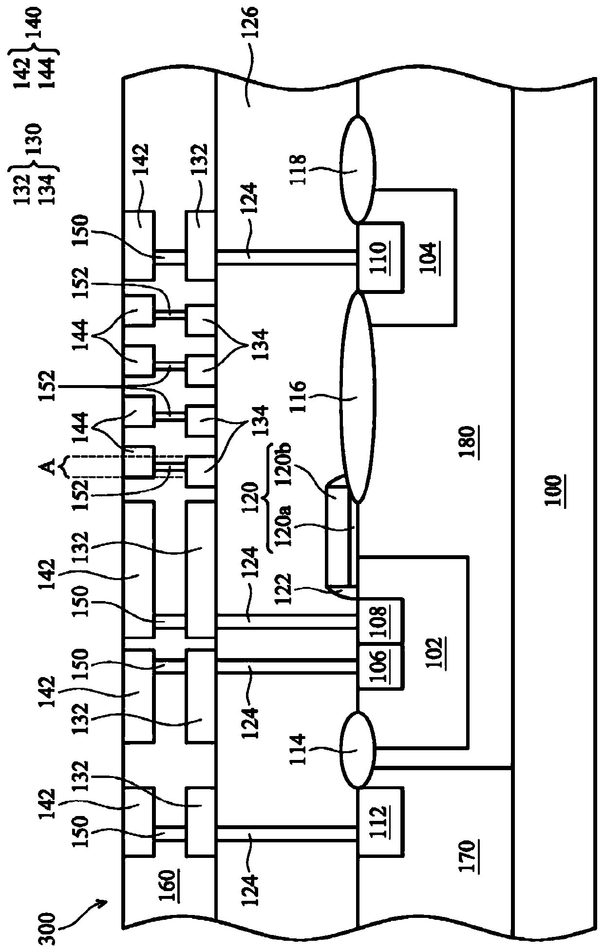
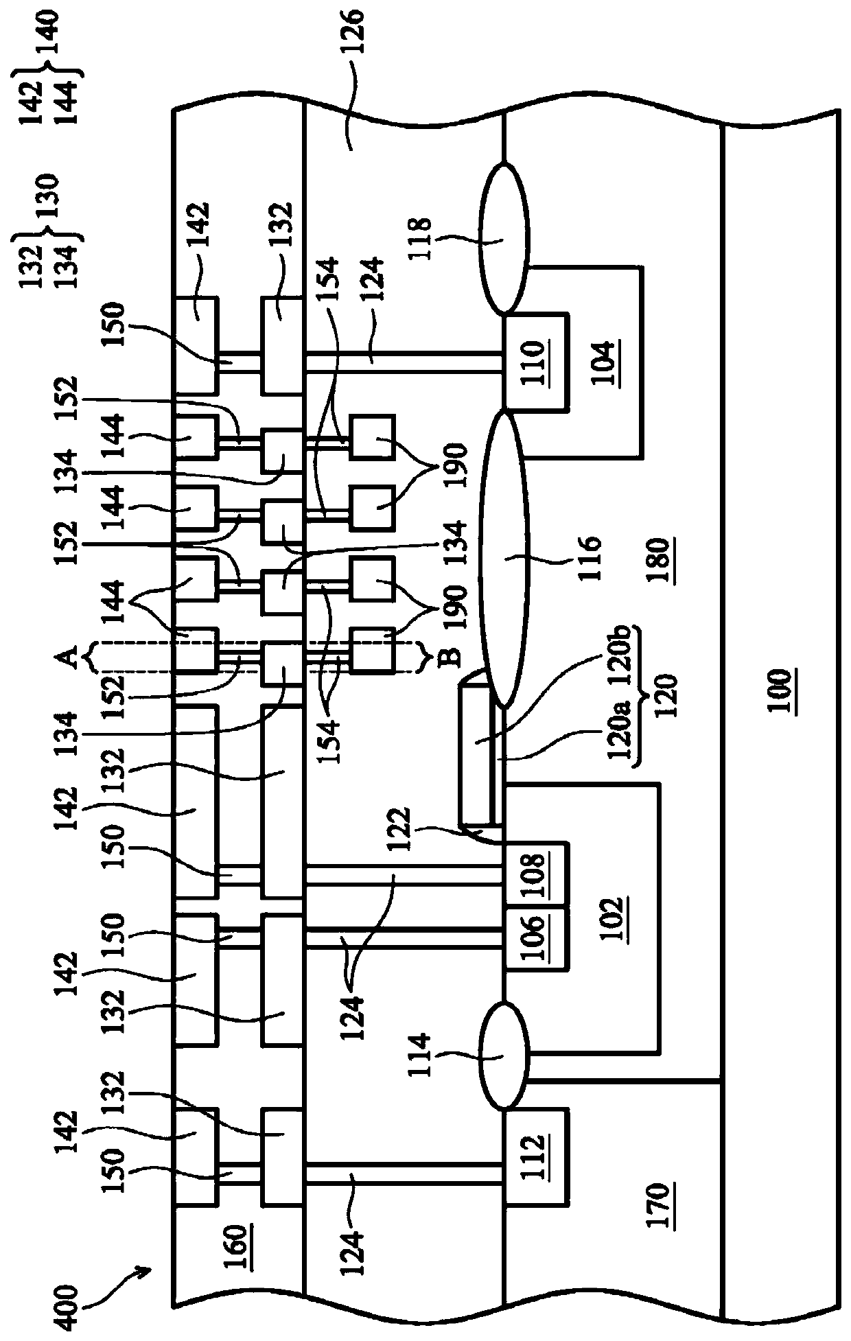
The invention provides a high voltage semiconductor device. The high-voltage semiconductor device comprises a substrate; a source electrode zone and a drain electrode are arranged in the substrate andare isolated by an isolation structure; the first metal layer is arranged on the substrate and comprises a first metal layer main body which is electrically connected to the source area and the drainarea and a plurality of first metal stop blocks which are arranged right above the isolation structure; the second metal layer is stacked on the first metal layer; the second metal layer main body iselectrically connected to the source zone or drain zone, and the plurality of second metal stop blocks are arranged right above the isolation structure, wherein a stacking part is arranged between each first metal stop block and the corresponding second metal block; a via hole is arranged between the first metal layer and the second metal layer; the via hole is arranged in a stacking part of thefirst metal stop block and the second metal stop block. The high voltage semiconductor device can prevent stray electrons from permeating to the isolation structure and can reduce rates of break through voltage drop and electricity leakage.

Description

technical field [0001] The present invention relates to semiconductor devices, and in particular to high voltage semiconductor devices. Background technique [0002] High-voltage semiconductor device technology is suitable for high-voltage and high-power integrated circuits. Conventional high-voltage semiconductor devices, such as vertically diffused metal oxide semiconductor (VDMOS) transistors and horizontally diffused metal oxide (LDMOS) transistors, are mainly used in device applications above 18V. The advantage of high-voltage semiconductor device technology is that it is cost-effective and easily compatible with other processes. It has been widely used in the fields of display driver IC components, power supplies, power management, communications, automotive electronics, or industrial control. [0003] In traditional high-voltage semiconductor devices, the isolation structure (such as a field oxide layer) is directly exposed under the protective layer or molding compo...

Claims


Application Information

Patent Timeline
Patent Type & Authority Patents(China)
IPC IPC(8): H01L29/78H01L29/06H01L21/768
CPCH01L21/76895H01L29/0611H01L29/0684H01L29/7815
Inventor 苏布陈柏安维克
Owner NUVOTON
Learn More