Efficient low-loss broadband waveguide-microstrip conversion device

A conversion device and low-loss technology, applied in the direction of connection devices, waveguide devices, electrical components, etc., can solve the problems of restricting mass production, reducing the qualified rate of finished products, and difficult processing, so as to reduce development and processing costs and hardware The waste of resources and the effect of high flexibility in use

Inactive Publication Date: 2018-02-13
BEIJING RES INST OF TELEMETRY +1
View PDF3 Cites 5 Cited by
  • Summary
  • Abstract
  • Description
  • Claims
  • Application Information

AI Technical Summary

Problems solved by technology

The probe conversion method has low insertion loss, small return loss, wide response bandwidth and compact structure, convenient processing, easy assembly and disassembly, and is a commonly used high-quality conversion method, but it needs to use multiple temperature gradients in the process of processing Welding, poor consistency, this shortcoming restricts mass production and will greatly reduce the qualified rate of finished products
[0007] In summary, the existing technology has disadvantages such as high cost, difficult processing, poor consistency, etc.

Method used


Image

  • Efficient low-loss broadband waveguide-microstrip conversion device
  • Efficient low-loss broadband waveguide-microstrip conversion device
  • Efficient low-loss broadband waveguide-microstrip conversion device

Examples


Embodiment Construction

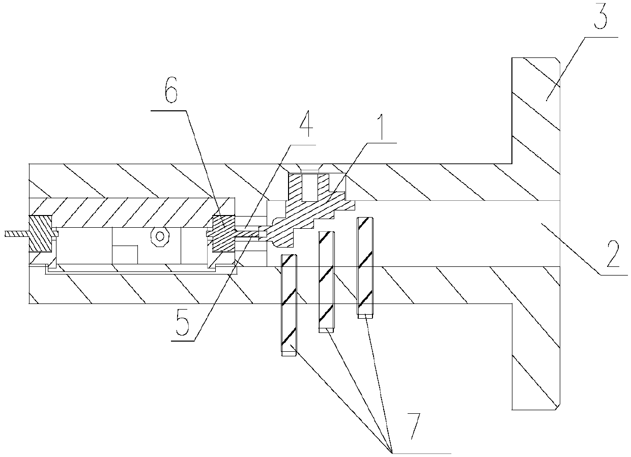
[0023] like figure 1 As shown in the figure, a high-efficiency, low-loss broadband waveguide-microstrip conversion device includes: a tail-feed ladder 1, a housing 3, a glass insulator 6, and a tuning screw 7; the housing 3 is connected to external equipment through a flange, and the internal The baffle divides the inner cavity of the shell 3 into two cavities, front and rear, and the end with the flange is the waveguide cavity 2;

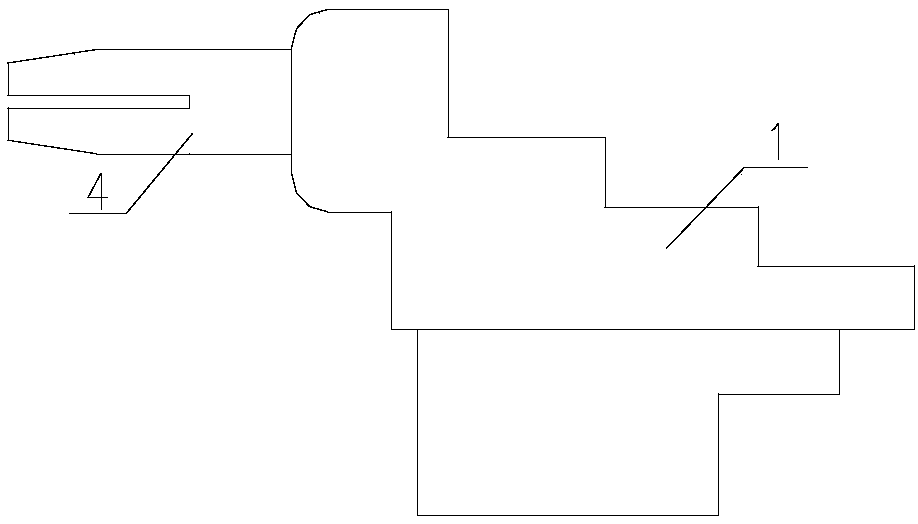
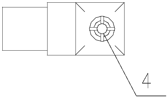
[0024] The tail-feed ladder 1 structure adopts a multi-stage ladder structure, which can achieve ultra-wideband response. The tail-feed ladder 1 has an integrated structure, including a stepped part, a cross-slot elastic interface 4 and a connecting part; one surface of the stepped part is a stepped surface, which is installed on the inner wall of the waveguide cavity 2 through the connecting part; the cross-slot elastic interface 4 is cylindrical, One end is processed with a cross groove, and the other end is connected to one side of the stepped ...


PUM


Abstract

Disclosed is an efficient low-loss broadband waveguide-microstrip conversion device. The conversion device comprises a tail feed ladder (1), a shell body (3), a glass insulator (6) and tuning screws (7); the tail feed ladder (1) is installed on the inner wall of a waveguide cavity (2) of the shell body (3), and a cross slot elastic interface (4) in the side surface is connected with the glass insulator (6); a pin (5) at one end of the glass insulator (6) is inserted into a cross slot in the end portion of the cross slot elastic interface (4), and the other end of the glass insulator (6) is connected with a circuit at the rear end; each tuning screw (7) is inserted from the side wall of the waveguide cavity (2) and is opposite to the step surface of the tail feed ladder (1). The conversiondevice overcomes the limitation of a traditional waveguide-microstrip conversion technology, a good standing-wave ratio, ground insertion loss and broadband response are obtained, the technical processing procedures are simplified, and good consistency is achieved at the same time.

Description

technical field [0001] The invention relates to a broadband waveguide-microstrip conversion device, which belongs to the field of communication radar. Background technique [0002] With the development of millimeter-wave integrated circuits, many application systems put forward the requirement of waveguide-to-microstrip conversion integrated with microstrip integrated circuits. Various indicators of waveguide microstrip conversion, such as standing wave ratio, insertion loss and response frequency width, directly affect the performance of the entire system, and its design and processing difficulty directly determines the possibility of process production. Therefore, the development of this technology has increasingly become the focus of attention. [0003] So far, there are three main methods of waveguide microstrip conversion: fin line conversion, ridge waveguide conversion, and probe conversion. [0004] Ridge-waveguide switching is a simple method with good transition c...

Claims


Application Information

Patent Timeline
Patent Type & Authority Applications(China)
IPC IPC(8): H01P5/107
CPCH01P5/107
Inventor 毕娜娜刘德喜祝大龙李保平刘星辰
Owner BEIJING RES INST OF TELEMETRY
Why Eureka
Try Eureka