Electric connection structure making method and integrated circuit chip

A technology for electrical connection structures and chips, applied in circuits, electrical components, electrical solid devices, etc., can solve problems that affect the yield and reliability, increase the stress of integrated circuit films, and warping of films, so as to improve reliability and Yield rate, avoiding aluminum-silicon mutual dissolution and other structural defects, suitable for mass production

Inactive Publication Date: 2018-01-16
PEKING UNIV FOUNDER GRP CO LTD +1
View PDF9 Cites 0 Cited by
  • Summary
  • Abstract
  • Description
  • Claims
  • Application Information

AI Technical Summary

Problems solved by technology

[0003] (1) The metal in the contact hole is in contact with the underlying silicon-based material, which may cause aluminum-silicon mutual dissolution, that is, the formation of metal silicide particles, which may increase the film stress of the integrated circuit, causing the film to warp or Structural defects such as unevenness;
[0004] (2) The metal in the contact hole is usually formed in the form of metal atoms, usually by metal sputtering, evaporation and electroplating, etc. The metal layer formed by the metal atoms may be discontinuous, which will cause the circuit break of the integrated circuit, which seriously affects Yield and Reliability

Method used


Image

  • Electric connection structure making method and integrated circuit chip
  • Electric connection structure making method and integrated circuit chip
  • Electric connection structure making method and integrated circuit chip

Examples


preparation example Construction

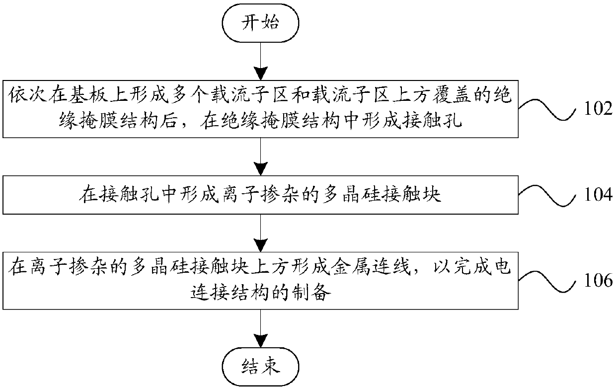
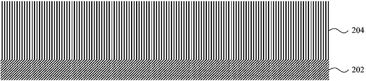
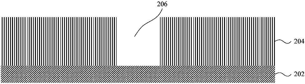
[0039] Such as figure 1 As shown, the method for preparing an electrical connection structure according to an embodiment of the present invention includes: step 102, after sequentially forming a plurality of carrier regions and an insulating mask structure covering the carrier regions on the substrate, Forming a contact hole in the film structure; Step 104, forming an ion-doped polysilicon contact block in the contact hole; Step 106, forming a metal connection on the ion-doped polysilicon contact block to complete the preparation of the electrical connection structure.

[0040] In this technical scheme, an ion-doped polysilicon contact block is formed in the contact hole, and a metal connection is formed above the ion-doped polysilicon contact block, thereby forming an electrical connection between the bottom carrier region and the top metal connection. contact, avoiding the filling of metal atoms in the contact hole, thereby avoiding the mutual dissolution of aluminum and sil...


PUM


Abstract

The invention provides an electric connection structure making method and an integrated circuit chip. The making method comprises steps: after multiple carrier areas and an insulated mask structure covering the carrier areas are sequentially formed on a substrate, a contact hole is formed in the insulated mask structure; an ion-doped polysilicon contact block is formed in the contact hole; and metal wiring is formed above the ion-doped polysilicon contact block to complete making of the electric connection structure. Through the technical scheme provided by the invention, the possibility of poor contact caused by mutual solubility of aluminum and silicon is reduced, the possibility of open circuit of the integrated circuit is further reduced, and the reliability of the circuit connection of the integrated circuit is enhanced.

Description

technical field [0001] The invention relates to the technical field of semiconductor chip manufacturing, in particular to a method for preparing an electrical connection structure and an integrated circuit chip. Background technique [0002] At present, according to the guidance of Moore's Law to the semiconductor industry, the research direction of integrated circuits is mainly miniaturization and integration. Filling metal in contact holes can have a number of drawbacks: [0003] (1) The metal in the contact hole is in contact with the underlying silicon-based material, which may cause aluminum-silicon mutual dissolution, that is, the formation of metal silicide particles, which may increase the film stress of the integrated circuit, causing the film to warp or Structural defects such as unevenness; [0004] (2) The metal in the contact hole is usually formed in the form of metal atoms, usually by metal sputtering, evaporation and electroplating, etc. The metal layer for...

Claims


Application Information

Patent Timeline
Patent Type & Authority Applications(China)
IPC IPC(8): H01L21/48H01L23/49
Inventor 贺冠中
Owner PEKING UNIV FOUNDER GRP CO LTD
Why Eureka
Try Eureka