Display panel, display panel preparation method, and display device
A technology for display panels and substrates, applied in semiconductor/solid-state device manufacturing, electrical components, electrical solid-state devices, etc., can solve problems such as incomplete exposure, short circuit of laminated metal lines, and uneven thickness of photoresist coating
- Summary
- Abstract
- Description
- Claims
- Application Information
AI Technical Summary
Problems solved by technology
Method used
Image
Examples
no. 1 example
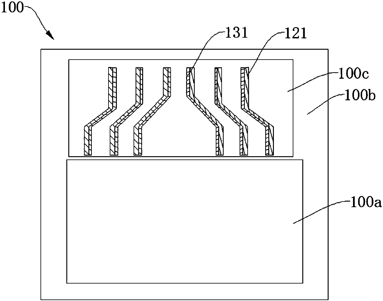
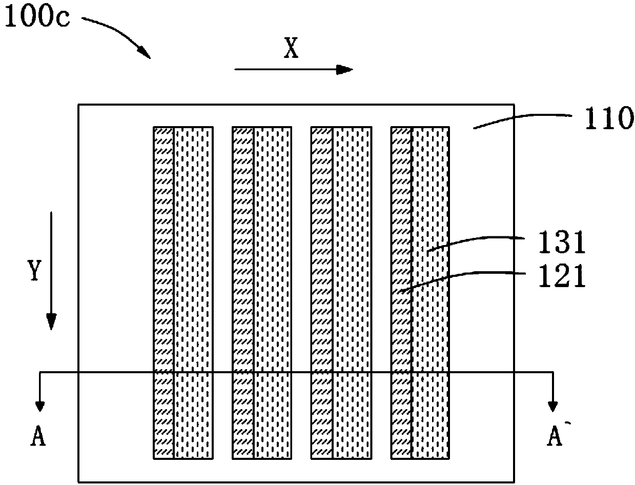
[0039] see Figure 4 and Figure 5 , the second metal line 131 is disposed on the insulating layer 140 , and the second metal line 131 partially falls within the first metal line 121 a in the orthographic projection area on the first metal layer 120 , and the other part falls into the first gap 122 area adjacent to the first metal line 121b area. The distance between the first metal lines 121a and 121b is L. During the preparation process of the second metal line 131, the mask 170 is shifted in the X direction from the position facing the first metal line 121 by a1, and a1 is less than L. After coating the photoresist 160 on the metal layer 150, aligning the mask 170 and photolithography, the second metal lines 131 are obtained, as shown in Figure 4 shown. At this time, there may be locally thick photoresist 160a at the recess 141 that is difficult to complete, and some metal 151 may remain. If the metal is completely removed, the short circuit between the second metal l...
no. 2 example
[0041] see Image 6 and Figure 7 , the second metal line 131 is disposed on the insulating layer 140 , and the second metal line 131 partially falls within the first metal line 121 a in the orthographic projection area on the first metal layer 120 , another part covers the first gap 122 adjacent to the first metal line 121a region, and another part falls into the first metal line 121b region adjacent to the first metal line 121a region. The distance between the first metal lines 121a, 121b is L. In the process of preparing the second metal line 131, the mask 170 is shifted along the X direction from the position facing the first metal line 121 by a2, and a2 is greater than L, and the width of the second metal line 131 is greater than that of the first metal line Spacing between 121a, 121b. In this embodiment, the second metal wire 131 spans the first gap 122 in the width direction. Preferably, the central axis of the second metal wire 131 may be collinear with the central ...
no. 3 example
[0043] see Figure 8 and Figure 9 , the second metal line 131 is disposed on the insulating layer 140, and the orthographic projection area of the second metal line 131 on the first metal layer 120 falls into the first metal line 121a and the adjacent between the first metal lines 121b. The distance between the first metal lines 121a, 121b is L. In the process of preparing the second metal line 131, the mask 170 is shifted along the X direction from the position facing the first metal line 121 by a3, and a3 is smaller than L, and the width of the second metal line 131 is smaller than that of the first metal line The distance between 121 a and 121 b , that is, the orthographic projection area of the second metal line 131 on the first metal layer 120 falls into the area of the first gap 122 . Preferably, the central axis of the second metal wire 131 may be collinear with the central axis of the first gap 122 , that is, two adjacent second metal wires may be arranged be...
PUM
 Abstract
Description
Claims
Application Information
 - R&D
- Intellectual Property
- Life Sciences
- Materials
- Tech Scout
- Unparalleled Data Quality
- Higher Quality Content
- 60% Fewer Hallucinations
Browse by: Latest US Patents, China's latest patents, Technical Efficacy Thesaurus, Application Domain, Technology Topic, Popular Technical Reports.
© 2025 PatSnap. All rights reserved.Legal|Privacy policy|Modern Slavery Act Transparency Statement|Sitemap|About US| Contact US: help@patsnap.com


