Metal interconnection structure, preparation method thereof and semiconductor device
A technology of metal interconnection structure and conductive layer, applied in semiconductor devices, semiconductor/solid-state device manufacturing, semiconductor/solid-state device components, etc., can solve problems such as poor barrier coverage, reduce short-circuit problems, and achieve good coverage Effect
- Summary
- Abstract
- Description
- Claims
- Application Information
AI Technical Summary
Problems solved by technology
Method used
Image

Examples
Embodiment 1
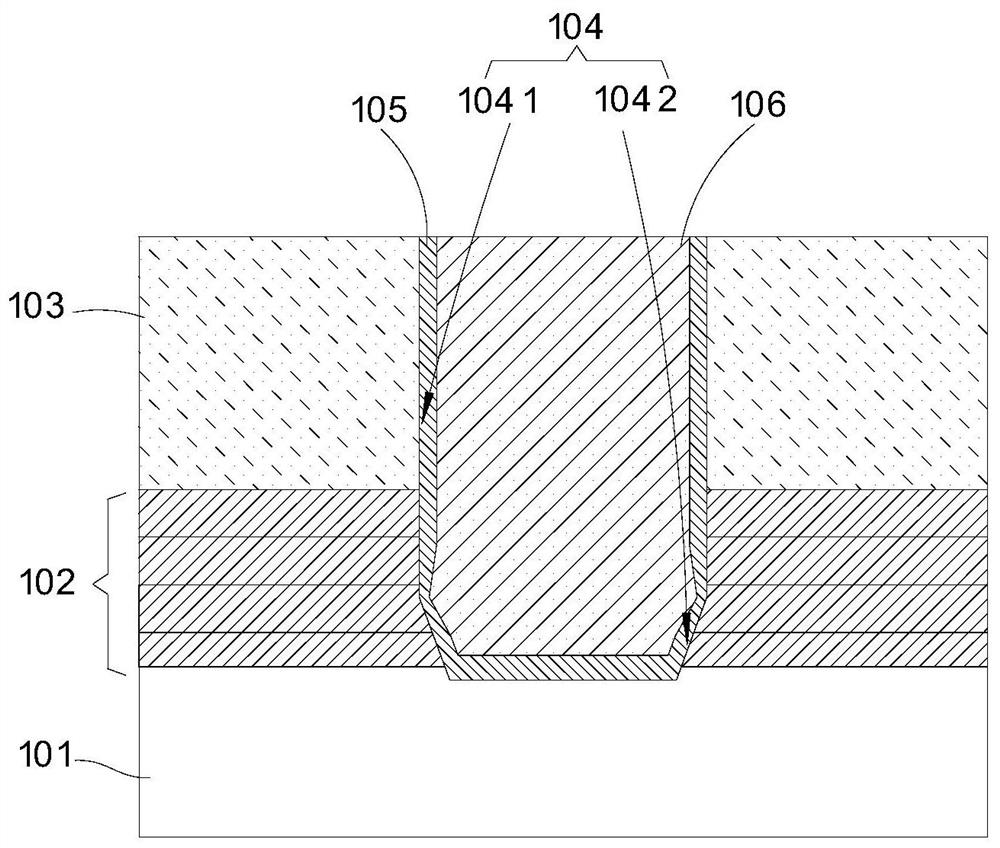
[0049] like figure 1 As shown, the embodiment of the present application provides a metal interconnection structure, including: a substrate 101 , an etching stop layer 102 , a protection layer 103 , a contact hole 104 , a diffusion barrier layer 105 and a conductive layer 106 .
[0050] An etch stop layer 102 is located above the substrate 101 . The etch stop layer 102 is used to prevent over-etching during the etching process of the contact hole 104 , and avoid damage to components under the contact hole 104 caused by over-etching.
[0051] The material of the etch stop layer 102 includes carbon-doped silicon nitride (NDC).
[0052] The etch stop layer 102 includes multi-layer stop layers stacked in sequence along a direction away from the substrate 101 .
[0053] In addition, the etch stop layer 102 also has a blocking function for preventing unwanted elements (eg, copper, tungsten, etc.) from diffusing into the protection layer 103 above it.
[0054] The passivation laye...
Embodiment 2
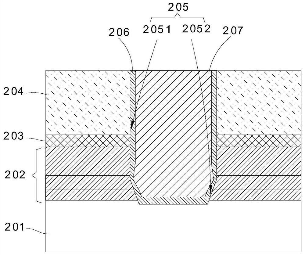
[0070] like image 3 As shown, the embodiment of the present application provides a metal interconnection structure, including: a substrate 201 , an etch stop layer 202 , an isolation layer 203 , a protection layer 204 , a contact hole 205 , a diffusion barrier layer 206 and a conductive layer 207 .
[0071] The etch stop layer 202 is located above the substrate 201 , and the etch stop layer 202 is used to prevent over-etching during the etching process of the contact hole 205 and avoid damage to components under the contact hole 205 due to over-etching.
[0072] The material of the etch stop layer 202 includes carbon-doped silicon nitride (NDC).
[0073] The etch stop layer 202 includes multi-layer stop layers stacked in sequence along a direction away from the substrate 201 .
[0074] In addition, the etch stop layer 202 also has a blocking function for preventing unnecessary elements (eg, copper, tungsten, etc.) from diffusing into the protective layer 204 above it.
[00...
Embodiment 3
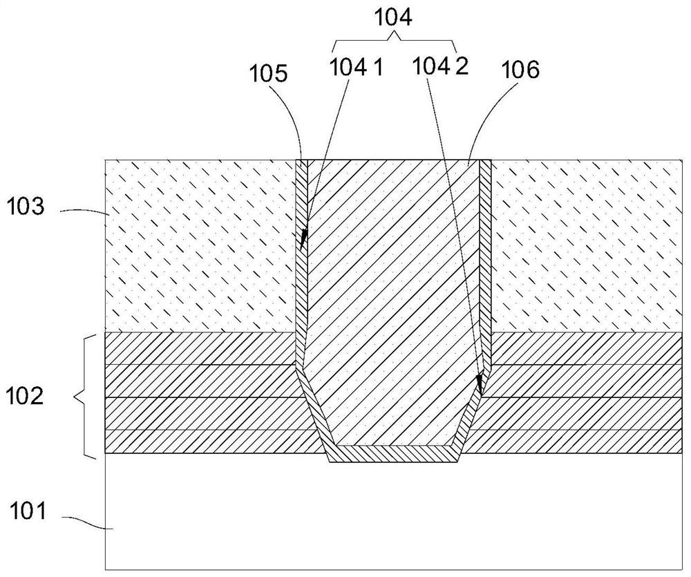
[0096] On the basis of Embodiment 1 or Embodiment 2, this embodiment provides a method for preparing a metal interconnection structure. Figure 5 It is a schematic flowchart of a method for preparing a metal interconnection structure shown in the embodiment of the present application. Figure 6-Figure 8 It is a schematic diagram of a cross-sectional structure formed by related steps of a method for preparing a metal interconnection structure shown in the embodiment of the present application. Below, refer to Figure 5 and Figure 6-Figure 8 The detailed steps of an exemplary method of the method for manufacturing the metal interconnection structure proposed in the embodiment of the present application will be described.
[0097] like Figure 5 As shown, the method for preparing the metal interconnection structure of this embodiment includes the following steps:
[0098] Step S110 : providing a substrate 101 .
[0099] Step S120: if Image 6 As shown, an etch stop layer 1...
PUM
 Abstract
Description
Claims
Application Information
 - R&D
- Intellectual Property
- Life Sciences
- Materials
- Tech Scout
- Unparalleled Data Quality
- Higher Quality Content
- 60% Fewer Hallucinations
Browse by: Latest US Patents, China's latest patents, Technical Efficacy Thesaurus, Application Domain, Technology Topic, Popular Technical Reports.
© 2025 PatSnap. All rights reserved.Legal|Privacy policy|Modern Slavery Act Transparency Statement|Sitemap|About US| Contact US: help@patsnap.com