


Quick Research
Generate reliable direction feasibility study reports for your R&D in just a few steps.

Technical Q&A
Discover and master advanced knowledge NOW. Basics, ideas, possibilities, all at once.

Find Solutions
As an expert in R&D theories, this can generate solutions to your technical problems instantly.

Evaluate Feasibility
Analyze your overall solution with one click, know your potential R&D risks in advance.

Monitor Landscape
Get weekly tech updates, stay abreast of the latest tech innovations and key insights.
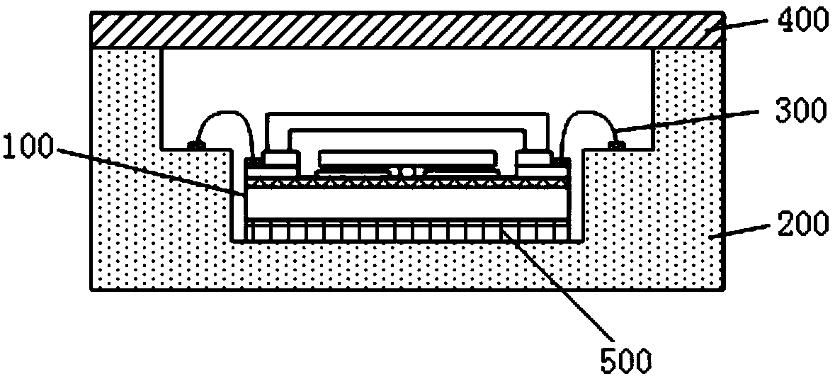
A method for manufacturing a center-supported mems chip packaging structure
A technology of chip packaging structure and center support, which is applied in the field of electronics, can solve the problems of increasing the total thickness of the device, increasing the complexity and cost of processing, and chip deformation, so as to increase the cost of packaging, increase the number and complexity of processing steps, and reduce stress. The effect of encapsulation
- Summary
- Abstract
- Description
- Claims
- Application Information
AI Technical Summary
Problems solved by technology
Method used
Image


Examples
Embodiment Construction
[0049] The present invention will be further described below in conjunction with the accompanying drawings. The following examples are only used to illustrate the technical solution of the present invention more clearly, but not to limit the protection scope of the present invention.
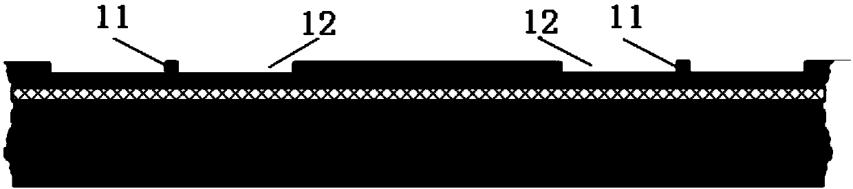
[0050] Traditional variable-pitch MEMS capacitive sensors such as figure 1 shown. The lower electrode of the MEMS capacitive sensor is directly fixed on the silicon dioxide isolation layer, and the silicon dioxide isolation layer is fixed on the silicon substrate. The upper electrode of the MEMS capacitive sensor (that is, the MEMS sensitive structural mass) is suspended on the lower electrode through the support of the central anchor point structure. The upper electrode and the lower electrode form a capacitance relative to each other. When there is an external sensitive quantity input, the capacitance value formed by the upper electrode and the lower electrode changes, and the detection of t...
PUM
 Abstract
Description
Claims
Application Information
 - R&D Engineer
- R&D Manager
- IP Professional
- Industry Leading Data Capabilities
- Powerful AI technology
- Patent DNA Extraction
Browse by: Latest US Patents, China's latest patents, Technical Efficacy Thesaurus, Application Domain, Technology Topic, Popular Technical Reports.
© 2024 PatSnap. All rights reserved.Legal|Privacy policy|Modern Slavery Act Transparency Statement|Sitemap|About US| Contact US: help@patsnap.com