Resonance temperature sensitive chip probe of isolation packaging structure and packaging method thereof

A technology for sensitive chips and packaging structures, applied in microstructure devices, manufacturing microstructure devices, microelectronics microstructure devices, etc., can solve problems such as performance degradation, increased pressure in the sealed cavity, sensor failure, etc., to improve long-term stability. , the effect of improving stability and increasing reliability

Active Publication Date: 2021-11-26
NO 49 INST CHINESE ELECTRONICS SCI & TECH GRP
View PDF5 Cites 0 Cited by
  • Summary
  • Abstract
  • Description
  • Claims
  • Application Information

AI Technical Summary

Problems solved by technology

[0007] The purpose of the present invention is to solve the problem that the existing resonant temperature sensitive chip is easily corroded, resulting in performance degradation or sensor failure
At the same time, due to the increase of leakage rate in the existing packaging method, the pressure in the sealed cavity increases, and there is a problem of decreased measurement accuracy and long-term stability.

Method used


Image

  • Resonance temperature sensitive chip probe of isolation packaging structure and packaging method thereof
  • Resonance temperature sensitive chip probe of isolation packaging structure and packaging method thereof
  • Resonance temperature sensitive chip probe of isolation packaging structure and packaging method thereof

Examples


specific Embodiment approach 1

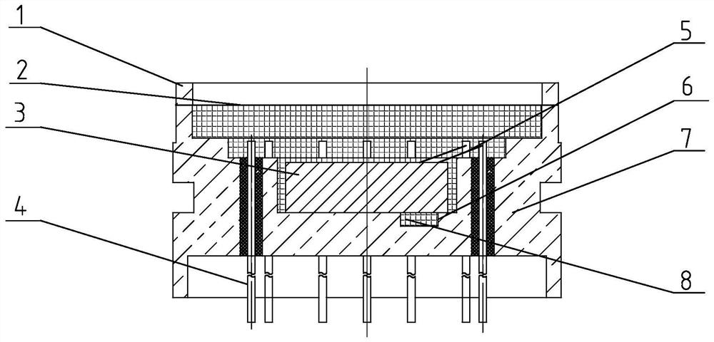
[0052] Specific implementation mode one: combine Figure 1 to Figure 8 Describe this embodiment, a resonant temperature-sensitive chip probe with an isolated package structure in this embodiment includes a pressure ring 1, a flat diaphragm 2, a silicon resonant temperature-sensitive chip 3, Kovar pins 4, electrode bonding wires 5, Probe medium transmission channel 6, sealing tube base 7 and isolation medium 8,

[0053] The silicon resonant temperature-sensitive chip 3 includes a chip upper cover 301, a resonant layer 302, a silicon-based substrate 3021, and a stress isolation layer 303. The chip upper cover 301, the resonant layer 302, the silicon-based substrate 3021, and the stress isolation layer 303 are arranged from top to bottom connected in turn and made into one body, the lower end surface of the silicon-based substrate 3021 is horizontal, wherein an absolute pressure chamber is formed between the chip upper cover 301 and the silicon-based substrate 3021, and the reson...

specific Embodiment approach 2

[0057] Specific implementation mode two: combination Figure 4 To describe this embodiment, a temperature-sensing through hole 3031 is opened in the middle of the stress isolation layer 303 of this embodiment. Such setting facilitates the transmission of pressure to the silicon-based substrate 3021 and then to the resonant layer 302 to achieve the purpose of pressure sensing. Other components and connections are the same as those in the first embodiment.

specific Embodiment approach 3

[0058] Specific implementation mode three: combination Figure 8 To illustrate this embodiment, the resonant layer 302 of this embodiment includes four extraction electrodes 3022, two driving electrodes 3023, a spare electrode 3024, two sensitive comb electrodes 3025, two stabilizing beams 3026, two transverse tension beams 3027, Anchor block 3028 and electrode channel 3029, two driving electrodes 3023 are arranged in parallel up and down, and an extraction electrode 3022 is installed on the left and right sides of each driving electrode 3023, and a sensitive comb electrode is installed on the opposite side of the two driving electrodes 3023 3025, a stabilizing beam 3026 is installed on the inner side of the two sensitive comb electrodes 3025, a transverse tension beam 3027 is respectively installed on the inner side of the two stabilizing beams 3026, and an anchor block 3028 is installed between the two transverse tension beams 3027, The anchor block 3028 is connected to the ...


PUM


Abstract

The invention relates to a probe and a packaging method thereof, in particular to a resonance temperature sensitive chip probe of an isolation packaging structure and a packaging method thereof. The invention aims to solve the problem that an existing resonant temperature sensitive chip is easy to corrode, so that the performance is reduced or a sensor fails. The existing packaging method has the problem that the measurement precision and the long-term stability are reduced. A kovar alloy pin is installed on a lead hole, a silicon resonance temperature sensitive chip is installed on a chip bonding surface, a gap is reserved between the silicon resonance temperature sensitive chip and the kovar alloy pin, and the silicon resonance temperature sensitive chip is connected with the kovar alloy pin through an electrode bonding lead. The flat diaphragm is mounted on the flat diaphragm contact surface, the compression ring is pressed on the flat diaphragm, and the isolation medium is filled in a closed cavity formed among the gap, the probe medium transfer channel, the flat diaphragm and the sealing tube seat. According to the packaging method, secondary packaging is carried out on the resonance layer, so that the silicon resonance temperature sensitive chip works in the isolation medium. The probe is used for temperature measurement and packaging of the temperature chip probe.

Description

technical field [0001] The invention relates to a resonant temperature-sensitive chip probe and a packaging method thereof, in particular to a resonant temperature-sensitive chip probe with an isolated packaging structure and a packaging method thereof, belonging to the field of MEMS resonant temperature sensors. Background technique [0002] Traditional temperature sensors such as thermocouples, platinum resistance thermometers, infrared temperature measurement, etc., generally have an accuracy of 0.15°C, which is not suitable for high-precision temperature measurement; if higher temperature measurement accuracy is required, an optical fiber temperature sensor is required, but the optical fiber temperature sensor is easy to wear and cost It is relatively high, mostly for multi-point distributed measurement, and has high technical requirements for optical fiber wiring. [0003] The silicon resonant temperature sensor indirectly measures the temperature by measuring the natur...

Claims


Application Information

Patent Timeline
Patent Type & Authority Applications(China)
IPC IPC(8): B81B7/00B81B7/02B81C1/00G01K7/00
CPCB81B7/0058B81B7/0045B81B7/02B81C1/00261B81C1/00325G01K7/00B81B2201/0278Y02P70/50
Inventor 刘兴宇孙权石庆国孟宪宁姜晓龙夏露
Owner NO 49 INST CHINESE ELECTRONICS SCI & TECH GRP
Why Eureka
Try Eureka