Photo-anode electrode material as well as preparation method and application thereof
A technology of electrode material and photoanode, applied in the direction of electrodes, chemical instruments and methods, electrolysis process, etc., can solve the problems of low sunlight utilization efficiency, small specific surface area, difficult application, etc., achieve enhanced photocatalytic performance and improve separation efficiency , the effect of increasing the contact area
- Summary
- Abstract
- Description
- Claims
- Application Information
AI Technical Summary
Problems solved by technology
Method used
Image
Examples
preparation example Construction
[0035] The invention provides a preparation method of the photoanode electrode material, comprising the following steps:
[0036] (1) depositing silver particles on the silicon substrate in a deposition solution to obtain a silver silicon substrate; the deposition solution is a mixed solution of silver nitrate and hydrogen fluoride;
[0037] (2) etching the silver silicon substrate in an etching solution to obtain an etching substrate; the etching solution is a mixture of hydrogen peroxide and hydrogen fluoride;
[0038] (3) dissolving the silver component in the etched substrate in a nitric acid solution to obtain a porous silicon substrate;
[0039] (4) soak the porous silicon substrate in the isopropanol solution of tetrabutyl titanate and absolute ethanol in sequence, repeat the soaking for 1 to 8 times to prepare a seed layer, and obtain Si-Ti(OH ) 4 Substrate;
[0040] (5) For the Si-Ti(OH) 4 The substrate is annealed to obtain Si-TiO 2 Substrate;
[0041] (6) the ...
Embodiment 1
[0059] With the n-type silicon wafer (111) whose resistivity range is 35Ω·cm as the silicon substrate, the silicon substrate is cleaned: first, the silicon substrate is immersed in 97wt% sulfuric acid and 30wt% sulfuric acid with a volume ratio of 3:1 Hydrogen peroxide for 20 minutes to remove organic residues and heavy metal ions on the surface of the silicon substrate. Afterwards, put the substrate together with the solution in the previous step into an ultrasonic cleaning machine at room temperature for ultrasonic cleaning at a frequency of 20KHz for 2 minutes, the number of times is 3 times, to peel off insoluble substances. Finally, put the substrate into deionized water for ultrasonic cleaning (20KHz) for 2 minutes and 3 times. The substrate was taken out, blown dry with nitrogen gas, and dried at 80° C. for 20 minutes in a blast drying oven.
[0060] Porous Si was prepared by metal-assisted chemical etching (MACE) based on a two-step method: the cleaned silicon substra...
Embodiment 2
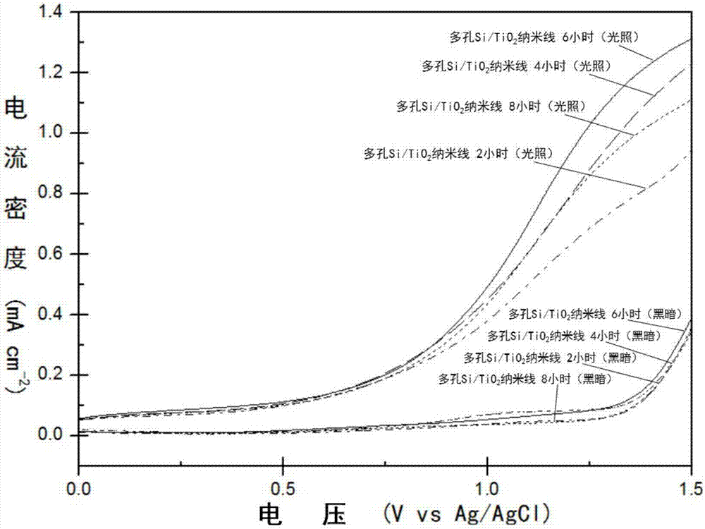
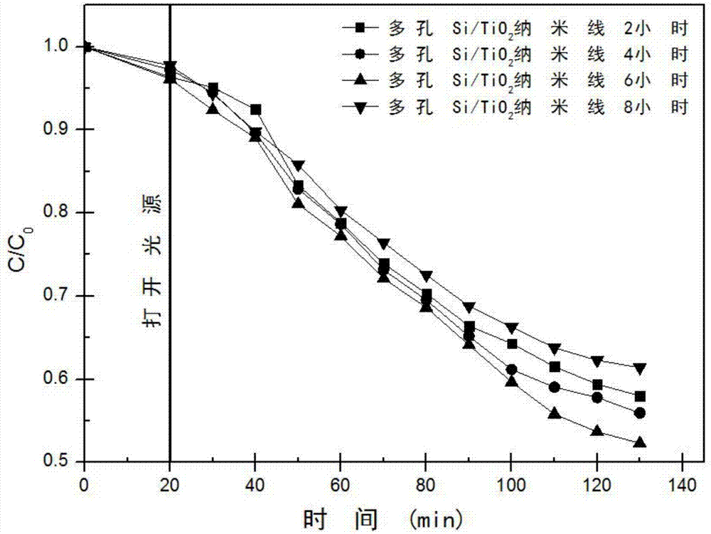
[0063] The crystal growth time was adjusted to 4 hours, and the rest of the steps and parameters were the same as in Example 1 to obtain the photoanode electrode material, marked as porous Si / SiO 2 Nanowires 4 hours.
PUM
| Property | Measurement | Unit |
|---|---|---|
| Resistivity | aaaaa | aaaaa |
| Concentration | aaaaa | aaaaa |
| Resistivity | aaaaa | aaaaa |
Abstract
Description
Claims
Application Information
 - R&D Engineer
- R&D Manager
- IP Professional
- Industry Leading Data Capabilities
- Powerful AI technology
- Patent DNA Extraction
Browse by: Latest US Patents, China's latest patents, Technical Efficacy Thesaurus, Application Domain, Technology Topic, Popular Technical Reports.
© 2024 PatSnap. All rights reserved.Legal|Privacy policy|Modern Slavery Act Transparency Statement|Sitemap|About US| Contact US: help@patsnap.com


