Circuit board and manufacturing method thereof

A manufacturing method and circuit board technology, which is applied in the fields of printed circuit manufacturing, circuit cover, printed circuit, etc., can solve the problems of unfavorable high-density circuit manufacturing and reduce the utilization rate of flexible circuit board typesetting, so as to increase the typesetting utilization rate and improve Effect of Yield and Aperture Reduction

Active Publication Date: 2020-05-22
AVARY HLDG (SHENZHEN) CO LTD +2
View PDF5 Cites 0 Cited by
  • Summary
  • Abstract
  • Description
  • Claims
  • Application Information

AI Technical Summary

Problems solved by technology

However, when making circuits, the holes on the flexible circuit board need to increase the hole ring to enhance its connection function, which reduces the utilization rate of the layout of the flexible circuit board, which is not conducive to the production of high-density circuits.

Method used


Image

  • Circuit board and manufacturing method thereof
  • Circuit board and manufacturing method thereof
  • Circuit board and manufacturing method thereof

Examples


Embodiment Construction

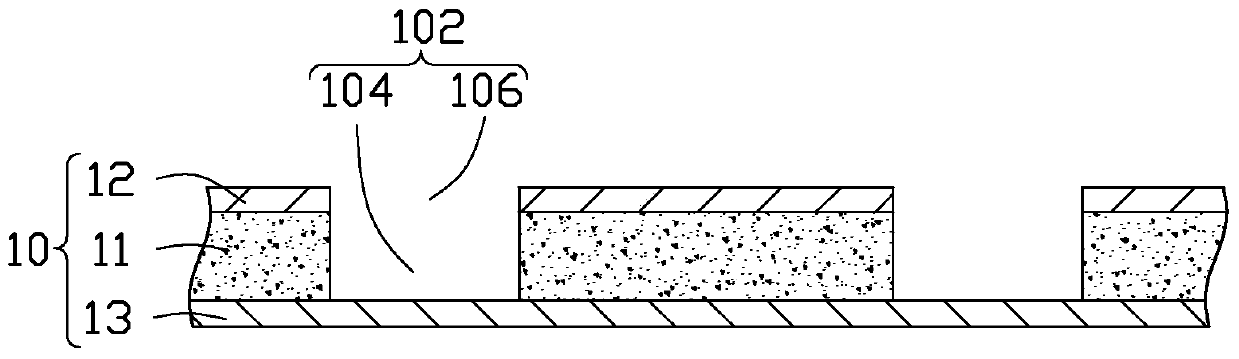
[0042] The following will be combined with Figure 1 to Figure 20 and an embodiment, the circuit board 100 provided by the technical solution and its manufacturing method are further described in detail. The circuit board 100 can be used in a high-density circuit board (HDI board), a rigid-flex board or a chip carrier board (IC carrier board).

[0043] see Figure 1 to Figure 8 , the first embodiment of the present invention provides a method for manufacturing a circuit board 100, including the following steps:

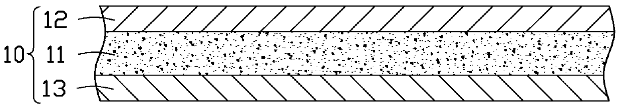
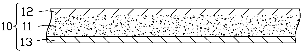
[0044] For a first step, see figure 1 , providing a substrate 10 .

[0045] The substrate 10 is double-sided, and the substrate 10 includes a base layer 11 , a first bottom copper layer 12 and a second bottom copper layer 13 formed on opposite sides of the base layer 11 .

[0046] In this embodiment, the base layer 11 is a flexible resin layer, such as polyimide (Polyimide, PI), polyethylene terephthalate (Polyethylene Terephthalate, PET) or polyethylene naphthala...


PUM


Abstract

A circuit board, comprising a base layer, a first conductive pattern layer and a second conductive pattern layer formed on both sides of the base layer, at least one conductive pattern layer is opened in the area of ​​the base layer not covered by the first conductive pattern layer Through the first hole of the base layer, the circuit board further includes a conductive circuit layer, the conductive circuit layer includes at least a first part and a second part connected to the first part, and the first part is filled in the first part. A hole, the second part protrudes from the first part toward the direction away from the base layer, the diameter of the second part is smaller than the diameter of the first hole, and the conductive circuit layer is electrically connected to the first A conductive pattern layer and a second conductive pattern layer.

Description

technical field [0001] The invention relates to a circuit board and a manufacturing method thereof. Background technique [0002] At present, many flexible circuit boards will have high complexity, high precision, and high density wiring requirements. However, during circuit fabrication, holes on the flexible circuit board need to be increased with rings to enhance their connection function, which reduces the utilization rate of flexible circuit board layout and is not conducive to the production of high-density circuits. Contents of the invention [0003] In view of this, the present invention provides a method for manufacturing a circuit board that avoids the existence of an annular structure. [0004] Also provided is a circuit board that avoids the presence of the annular ring structure. [0005] A method for manufacturing a circuit board, comprising the steps of: [0006] A substrate is provided, the substrate includes a base layer, a first bottom copper layer and ...

Claims


Application Information

Patent Timeline
Patent Type & Authority Patents(China)
IPC IPC(8): H05K1/11H05K3/40
CPCH05K1/115H05K3/4038H05K2201/096H05K3/108H05K3/427H05K2201/0367H05K2201/098H05K2201/09845H05K2203/0353H05K1/0298H05K1/09H05K3/0011H05K3/0073H05K3/02H05K3/4644H05K2201/095
Inventor 李艳禄杨梅李成佳
Owner AVARY HLDG (SHENZHEN) CO LTD
Why Eureka
Try Eureka