Semiconductor packaging device, semiconductor lead frame and rib-cutting method thereof

A packaging device and lead frame technology, applied in semiconductor devices, semiconductor/solid-state device manufacturing, semiconductor/solid-state device components, etc., can solve problems such as unreliable welding, poor soldering performance between pins and PCB printed circuit boards, etc. Achieve the effect of strengthening welding strength, improving welding performance and reliability

Pending Publication Date: 2017-10-20
SHENZHEN STS MICROELECTRONICS CO LTD
View PDF8 Cites 4 Cited by
  • Summary
  • Abstract
  • Description
  • Claims
  • Application Information

AI Technical Summary

Problems solved by technology

[0003] In order to solve the problems of poor welding performance and unreliable welding between the pins of the semiconductor packaging device and the PCB printed circuit board existing in the prior art, the present invention provides a semiconductor packaging device

Method used


Image

  • Semiconductor packaging device, semiconductor lead frame and rib-cutting method thereof
  • Semiconductor packaging device, semiconductor lead frame and rib-cutting method thereof
  • Semiconductor packaging device, semiconductor lead frame and rib-cutting method thereof

Examples


Embodiment Construction

[0043] In order to further illustrate the principle and structure of the present invention, preferred embodiments of the present invention will now be described in detail with reference to the accompanying drawings.

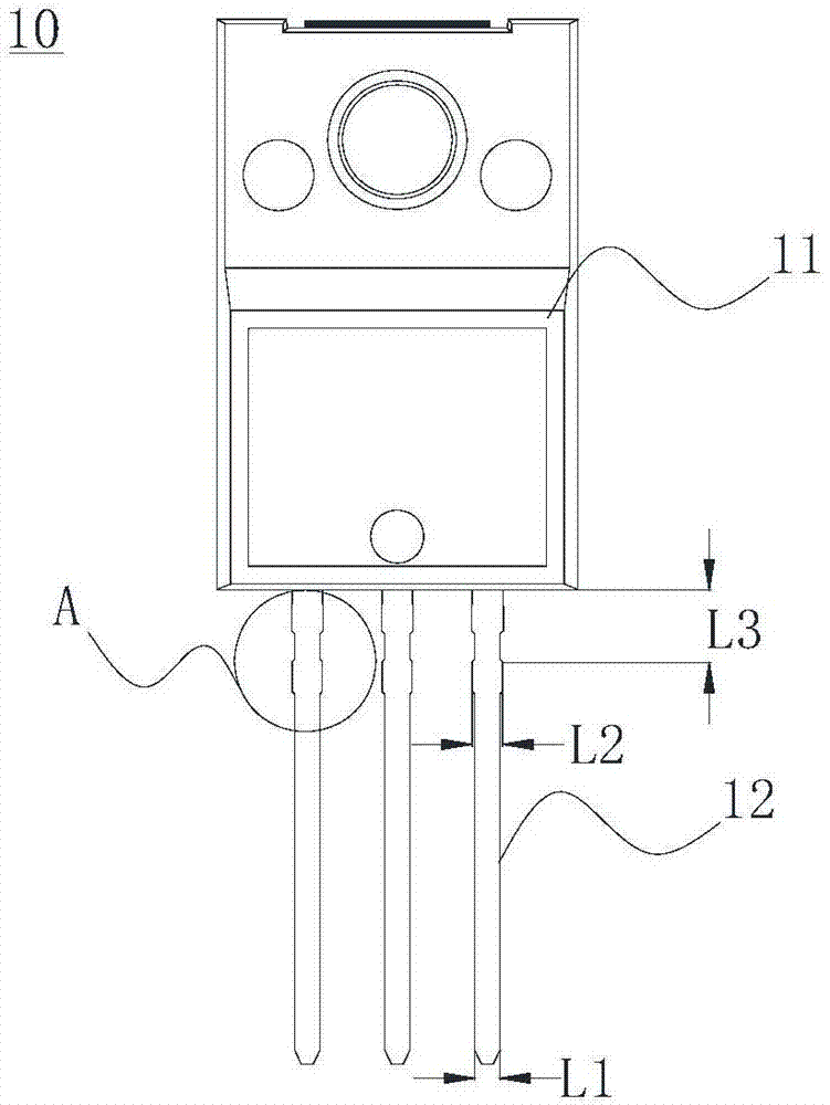
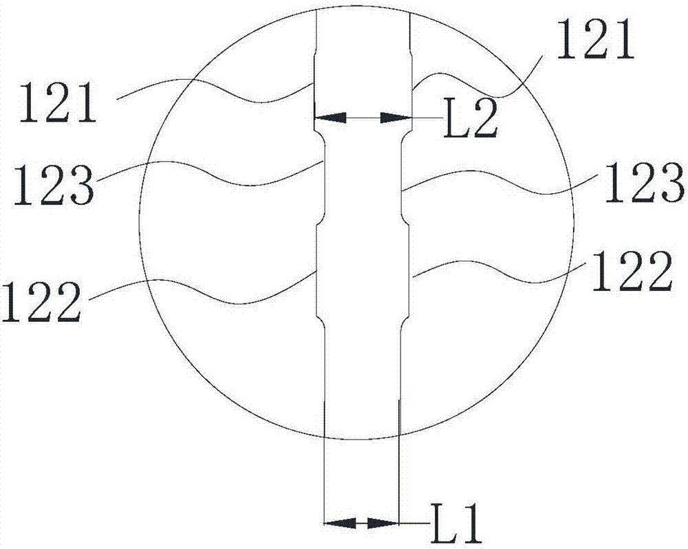
[0044] Such as figure 1 As shown, it is a schematic structural view of the semiconductor packaging device of the present invention. The package device 10 includes a package case 11 , a semiconductor device (not shown) wrapped in the package case 11 and pins 12 exposed outside the package case 11 .

[0045] exist figure 1 Wherein, the semiconductor packaging device may be a transistor packaging device, for example, a triode packaging device, and the transistor packaging device has three pins, which can be respectively connected to the gate, source and drain of the triode. But not limited thereto, the semiconductor packaging device can also be applied to the packaging of other semiconductor devices, for example, diodes, integrated chips, and the like. The number...


PUM


Abstract

The invention discloses a semiconductor packaging device, a semiconductor lead frame and a rib-cutting method thereof. The semiconductor packaging device comprises a packaging housing; a semiconductor device encapsulated in the packaging housing; and pins to be electrically connected with the semiconductor device and exposed out of the packaging housing. The two side, adjacent to the packaging housing, of each pin have square-wave structures each formed by two protrusions and a groove. The protrusions and the grooves are arranged successively and alternately along the length direction of the pin. When the pins and a PCB are soldered, soldering tin gathers in the grooves. The semiconductor lead frame and the rib-cutting method thereof are used for manufacturing the semiconductor packaging device. The semiconductor packaging device, the lead frame and the rib-cutting method thereof can improve the soldering performance and reliability of the pin and the PCB.

Description

technical field [0001] The invention relates to the packaging field of semiconductors, in particular to a semiconductor packaging device, a semiconductor lead frame and a rib cutting method thereof. Background technique [0002] A semiconductor packaging device is a device with an independent chip obtained by processing a wafer according to the product model and functional requirements. At present, the dimensions of the pins of semiconductor packaging devices, such as triode packaging devices, are generally 1.35 mm wide and 0.5 mm thick. When the semiconductor packaging device is mounted on a PCB printed circuit board, the occupied area of ​​the PCB printed circuit board is generally 1.35mm*0.5mm*3 (where 3 is the number of pins). For the in-line package, the PCB The printed circuit board needs to open a hole for each pin of the semiconductor packaging device, and the larger the pin, the larger the size of the hole, and the larger the size of the PCB printed circuit board, ...

Claims


Application Information

Patent Timeline
Patent Type & Authority Applications(China)
IPC IPC(8): H01L23/495H01L21/48
CPCH01L21/4842H01L23/49548H01L23/49562
Inventor 徐亚亚余蓥军杨晓东都俊兴周杰
Owner SHENZHEN STS MICROELECTRONICS CO LTD
Why Eureka
Try Eureka