


Quick Research
Generate reliable direction feasibility study reports for your R&D in just a few steps.

Technical Q&A
Discover and master advanced knowledge NOW. Basics, ideas, possibilities, all at once.

Find Solutions
As an expert in R&D theories, this can generate solutions to your technical problems instantly.

Evaluate Feasibility
Analyze your overall solution with one click, know your potential R&D risks in advance.

Monitor Landscape
Get weekly tech updates, stay abreast of the latest tech innovations and key insights.
Ultrathin and semitransparent thin film solar cell and preparation method thereof
A technology of solar cells and transparent conductive films, applied in circuits, photovoltaic power generation, electrical components, etc., can solve problems such as poor interface contact between the passivation layer and the back electrode, affecting battery performance, etc., to eliminate surface dangling bonds and reduce short circuits The effect of reducing the current density and increasing the transmittance
- Summary
- Abstract
- Description
- Claims
- Application Information
AI Technical Summary
Problems solved by technology
Method used
Image

Examples
Embodiment 1
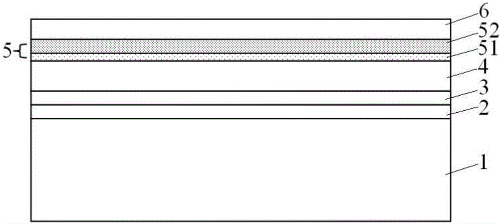
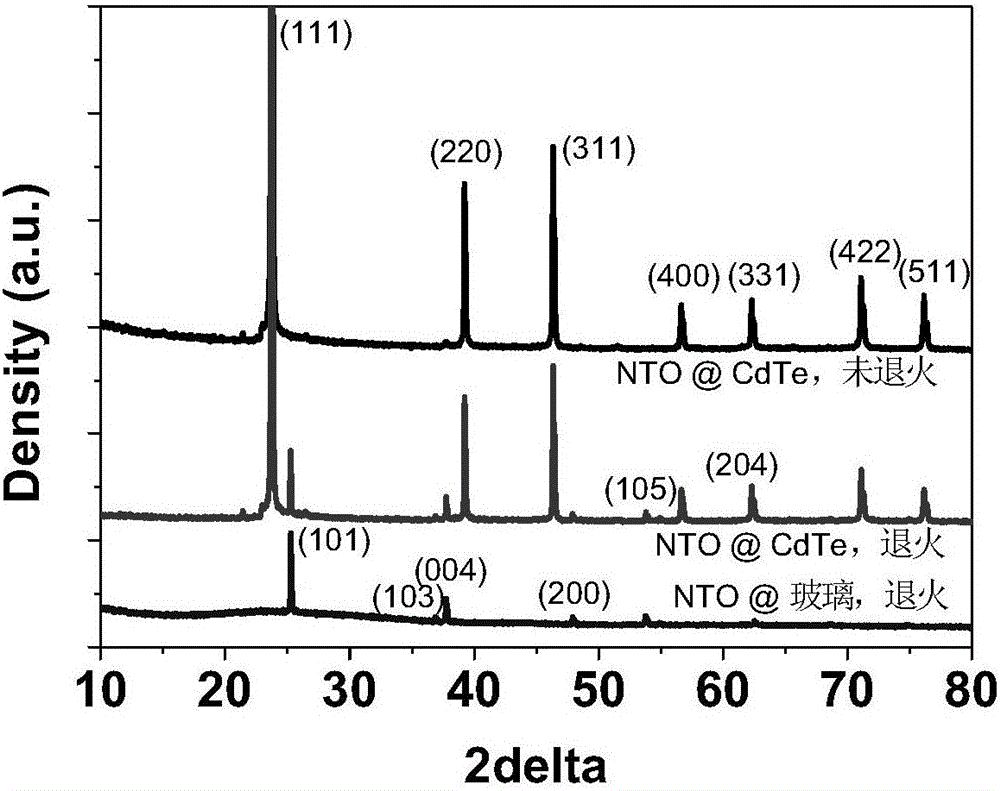
[0038] The ultra-thin translucent thin-film solar cell of this example, such as figure 1 As shown, it consists of a glass substrate 1 , a transparent conductive film layer 2 , an N-type transition layer 3 , a light absorbing layer 4 , a passivation layer 5 and a back electrode 6 stacked in sequence. The passivation layer 5 is a copper-doped semiconductor layer; the back electrode 6 is an NTO conductive film, that is, a niobium-doped titanium oxide layer; the light-absorbing layer in this example is a CdTe film. Wherein, the copper-doped semiconductor layer is formed by doping copper in the precursor thin film layer, that is, the precursor thin film layer 51 is deposited on the light absorbing layer 4, and the Cu film 52 is deposited on the precursor thin film layer 51, and then annealed to make the copper doped In the precursor thin film layer 51, form the passivation layer 5 of copper-doped semiconductor layer, and the precursor thin film layer is aluminum oxide layer, alumin...
Embodiment 2
[0047] The structure of the ultra-thin translucent thin-film solar cell of this example is the same as that of Example 1, and the thickness and specific preparation method of each layer are as follows:
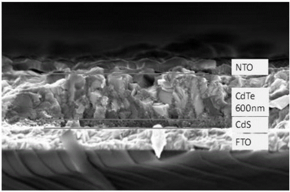
[0048] First, use the sputtering method to prepare a transparent conductive layer FTO with a thickness of 200nm-1000nm on the glass substrate, and sputter an N-type transition layer CdS with a thickness of 50-300nm on the transparent conductive layer FTO. In this example, a 200nm Transparent conductive layer FTO and 50nm N-type transition layer CdS; use near-vacuum evaporation to deposit CSS on the surface of N-type transition layer CdS to prepare a p-type CdTe light-absorbing layer with a thickness of 600nm; then, sequentially carry out CdCl 2 Annealing treatment, nitric acid phosphoric acid NP etching, the film with a certain amount of dangling bonds on the surface is obtained. Among them, sputtering, near-vacuum evaporation, CdCl 2 The annealing treatment and nitric acid p...
Embodiment 3
[0055] The structure of the ultra-thin translucent thin-film solar cell of this example is the same as that of Example 1, and the thickness and specific preparation method of each layer are as follows:
[0056] First, use the sputtering method to prepare a transparent conductive layer FTO with a thickness of 200nm-1000nm on the glass substrate, and sputter an N-type transition layer CdS with a thickness of 50-300nm on the transparent conductive layer FTO. In this example, a 1000nm Transparent conductive layer FTO and 300nm N-type transition layer CdS; use near-vacuum evaporation to deposit CSS on the surface of N-type transition layer CdS to prepare a p-type CdTe light-absorbing layer with a thickness of 800nm; then, sequentially carry out CdCl 2 Annealing treatment, nitric acid phosphoric acid NP etching, the film with a certain amount of dangling bonds on the surface is obtained.
[0057] Then, on the surface of the CdTe light-absorbing layer, Al 2 o 3 layer, the atomic la...
PUM
| Property | Measurement | Unit |
|---|---|---|
| thickness | aaaaa | aaaaa |
| thickness | aaaaa | aaaaa |
| thickness | aaaaa | aaaaa |
Abstract
Description
Claims
Application Information
 - R&D Engineer
- R&D Manager
- IP Professional
- Industry Leading Data Capabilities
- Powerful AI technology
- Patent DNA Extraction
Browse by: Latest US Patents, China's latest patents, Technical Efficacy Thesaurus, Application Domain, Technology Topic, Popular Technical Reports.
© 2024 PatSnap. All rights reserved.Legal|Privacy policy|Modern Slavery Act Transparency Statement|Sitemap|About US| Contact US: help@patsnap.com