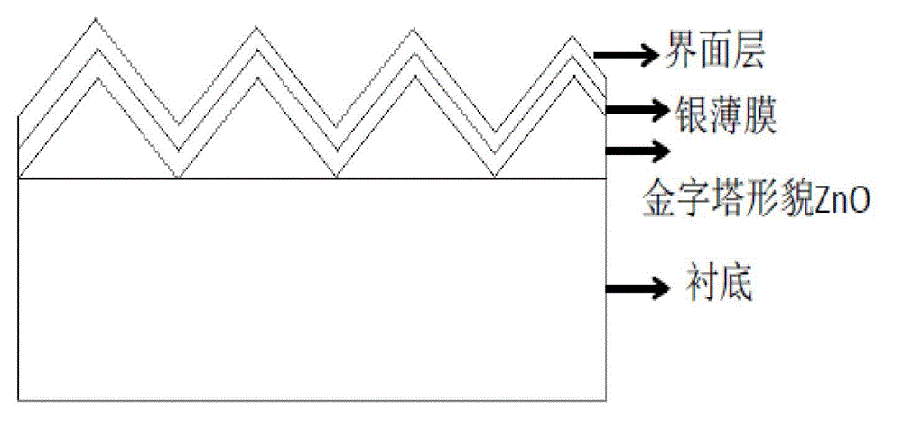
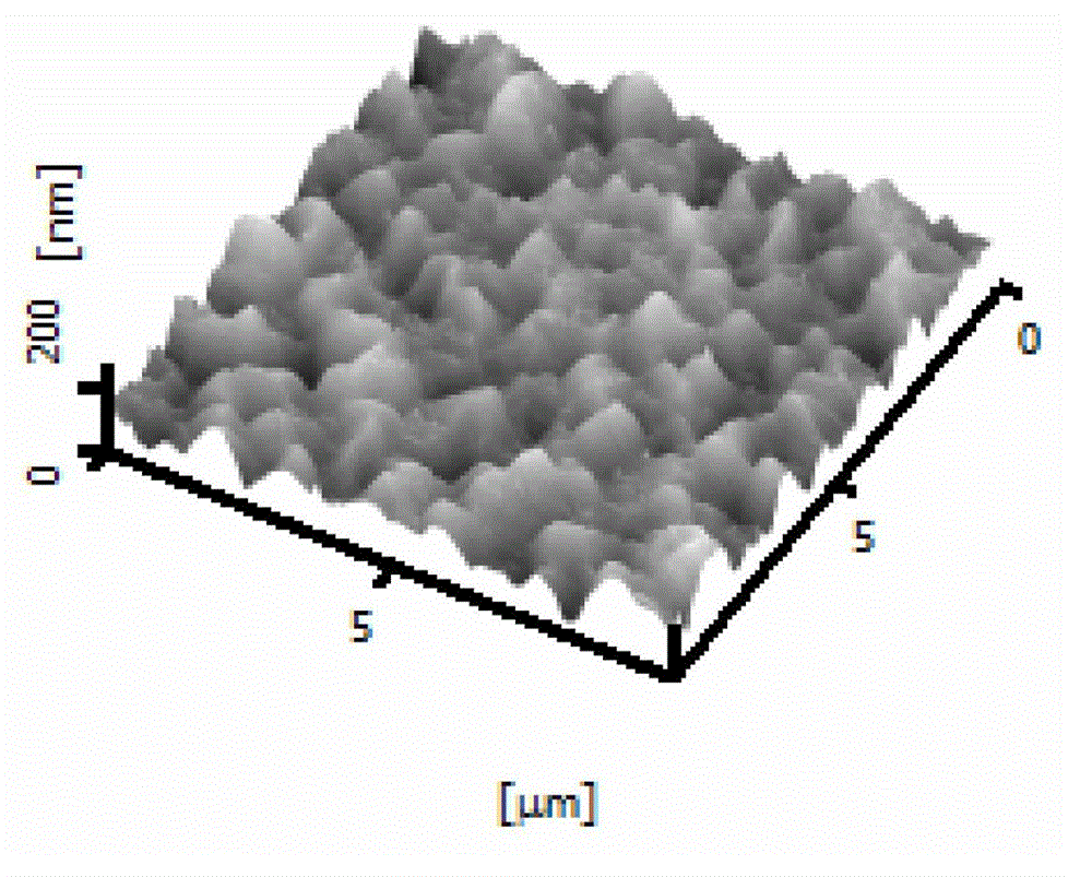
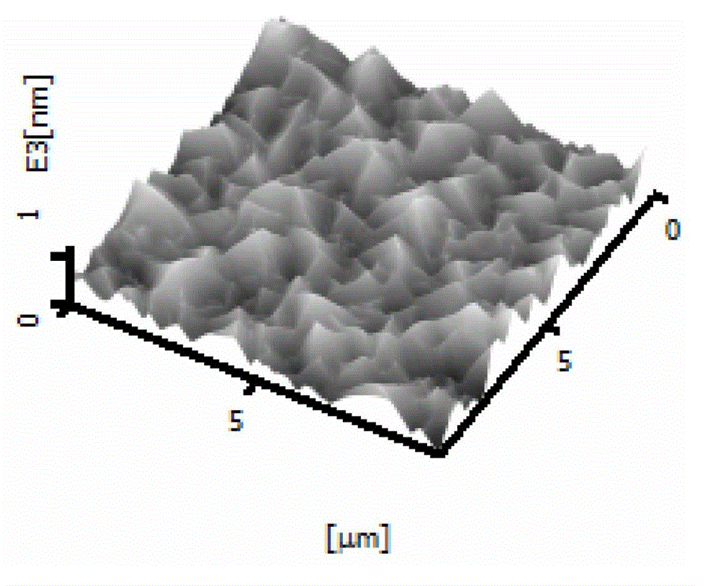
Conductive back reflection electrode based on pyramid texture degree morphology ZnO layer
A pyramid, back reflection technology, applied in circuits, electrical components, semiconductor devices, etc., can solve the problems of integral reflection characteristics and small velvet factor.
- Summary
- Abstract
- Description
- Claims
- Application Information
AI Technical Summary
Problems solved by technology
Method used
Image
Examples
Embodiment 1
[0022] A kind of preparation method based on the conductive back reflection electrode of pyramid velvet morphology ZnO layer, the steps are as follows:
[0023] 1) ZnO thin films were prepared on a clean glass substrate by metal-organic chemical vapor deposition technology, the heating temperature was 175°C, and the background vacuum was 5×10 -4 Pa, the flow rate of argon gas is 55 sccm, the reaction pressure is 1.2 Torr, the gas flow rate of water vapor and argon is 110 sccm, the flow rate of diethyl zinc and argon is 180 sccm, the growth time is 50 min, and the intrinsic ZnO with a thickness of 3000nm is transparent Conductive film;
[0024] 2) On the ZnO thin film layer with a pyramid structure surface morphology prepared above, a silver thin film layer with a thickness of 160nm is deposited by evaporation;
[0025] 3) On the above-mentioned silver thin film layer, a layer of ZnO thin film with a thickness of 100 nm is deposited as an interface layer by magnetron sputterin...
Embodiment 2
[0030] A kind of preparation method based on the conductive back reflection electrode of pyramid velvet morphology ZnO layer, the steps are as follows:
[0031] 1) The ZnO thin film was grown on a clean glass substrate by ultrasonic spray technology, zinc acetate was used as the Zn source, water and absolute ethanol were mixed at a volume ratio of 1:3 as a solvent, and zinc acetate was configured to 0.2mol / L solution, while adding 10vol.% glacial acetic acid, the growth temperature is 470°C, compressed air is used as the carrier gas, the growth time is 200min, and an intrinsic ZnO transparent conductive film with a thickness of about 5000nm is obtained;
[0032] 2) On the ZnO thin film layer with a pyramid structure surface morphology prepared above, a silver thin film layer with a thickness of 120nm is deposited by evaporation;
[0033] 3) On the above-mentioned silver thin film layer, a layer of ZnO thin film with a thickness of 100 nm is deposited as an interface layer by ...
Embodiment 3
[0036] A kind of preparation method based on the conductive back reflection electrode of pyramid velvet morphology ZnO layer, the steps are as follows:
[0037] 1) ZnO thin films were prepared on a clean glass substrate by metal-organic chemical vapor deposition technology, the heating temperature was 175°C, and the background vacuum was 5×10 -4 Pa, the flow rate of argon gas is 55 sccm, the reaction pressure is 1.0 Torr, the gas flow rate of water vapor and argon is 110 sccm, the flow rate of diethyl zinc and argon is 180 sccm, the growth time is 70 min, and the intrinsic ZnO with a thickness of 5000nm is transparent Conductive film;
[0038] 2) On the above-prepared ZnO thin film layer with a pyramid structure surface morphology, a silver thin film layer with a thickness of 150nm is deposited by evaporation;
[0039] 3) On the above-mentioned silver thin film layer, a layer of ZnO thin film with a thickness of 100 nm is deposited as an interface layer by magnetron sputterin...
PUM
| Property | Measurement | Unit |
|---|---|---|
| Root mean square roughness | aaaaa | aaaaa |
| Thickness | aaaaa | aaaaa |
| Thickness | aaaaa | aaaaa |
Abstract
Description
Claims
Application Information
 - R&D
- Intellectual Property
- Life Sciences
- Materials
- Tech Scout
- Unparalleled Data Quality
- Higher Quality Content
- 60% Fewer Hallucinations
Browse by: Latest US Patents, China's latest patents, Technical Efficacy Thesaurus, Application Domain, Technology Topic, Popular Technical Reports.
© 2025 PatSnap. All rights reserved.Legal|Privacy policy|Modern Slavery Act Transparency Statement|Sitemap|About US| Contact US: help@patsnap.com


