


Quick Research
Generate reliable direction feasibility study reports for your R&D in just a few steps.

Technical Q&A
Discover and master advanced knowledge NOW. Basics, ideas, possibilities, all at once.

Find Solutions
As an expert in R&D theories, this can generate solutions to your technical problems instantly.

Evaluate Feasibility
Analyze your overall solution with one click, know your potential R&D risks in advance.

Monitor Landscape
Get weekly tech updates, stay abreast of the latest tech innovations and key insights.
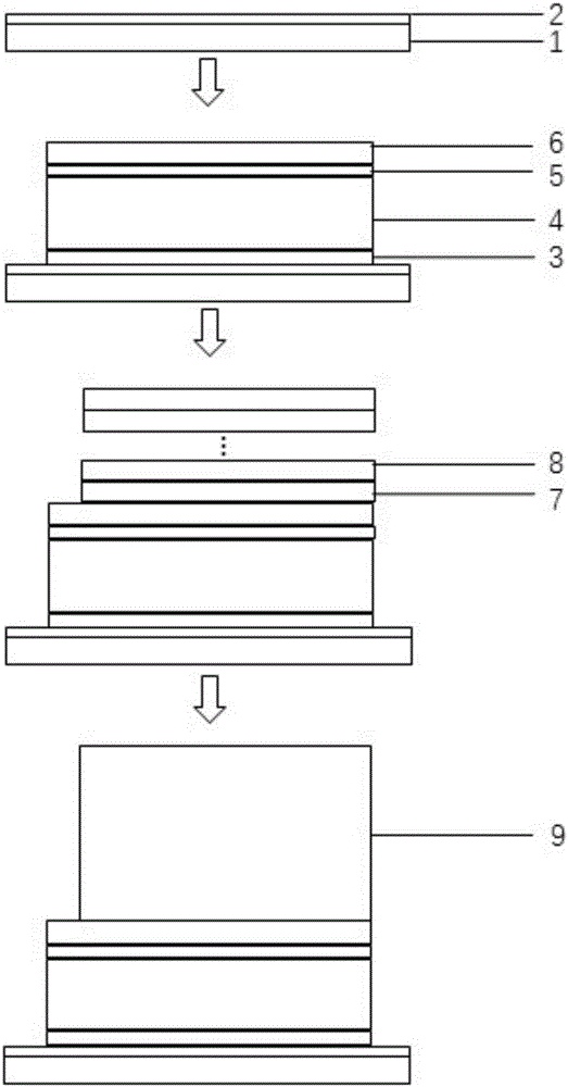
Preparation method of CIGS absorbing layer film doped with alkaline metal elements
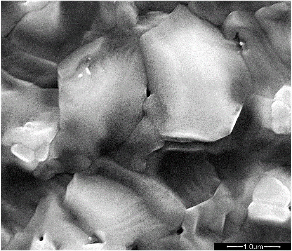
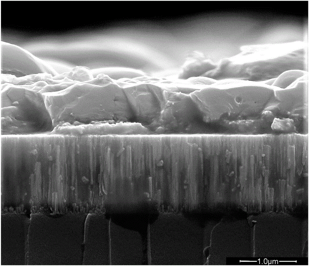
A metal element, copper indium gallium selenide technology, applied in electrical components, photovoltaic power generation, circuits, etc., can solve the problems of uneven mixing of elements, uneven distribution of elements, and large roughness of prefabricated layers, so as to achieve good crystallinity and maintain Integrity, bandgap adjustable effect
- Summary
- Abstract
- Description
- Claims
- Application Information
AI Technical Summary
Problems solved by technology
Method used
Image

Examples
Embodiment 1
[0060] (1) firstly make a silicon nitride barrier layer on a soda-lime glass substrate;
[0061] (2) Then deposit the back contact Mo layer on the substrate. First, the substrate is introduced into the sputtering deposition equipment, and after the equipment is closed, the vacuum is lowered to less than 4×10 -4 Pa; the first step is to deposit a high-resistance Mo layer after pre-sputtering the Mo target. The target is selected as a high-purity Mo target, the air pressure is selected at 0.6Pa, and the power density is maintained at 4W / cm 2 , the sputtering time is 10 minutes; the second step is to deposit a low-resistance Mo layer, the target is selected as a high-purity Mo target, the air pressure is selected at 0.1Pa, and the power density is maintained at 4W / cm 2 , the sputtering time is 60 minutes; the third step is to deposit the layer doped with alkali metal elements, the target material is selected as the target material doped with NaF, in which Na 2.5at%, the sputterin...
Embodiment 2
[0065] (1) firstly make a silicon nitride barrier layer on a soda-lime glass substrate;
[0066] (2) Then deposit the back contact Mo layer on the substrate. First, the substrate is introduced into the sputtering deposition equipment, and after the equipment is closed, the vacuum is lowered to less than 4×10 -4 Pa, the first step is to pre-sputter the Mo target and then deposit a high-resistance Mo layer. The target is selected as a high-purity Mo target, the air pressure is selected at 0.6Pa, and the power density is maintained at 4W / cm 2 , the sputtering time is 10 minutes, the second step is to deposit a low-resistance Mo layer, the target is selected as a high-purity Mo target, the air pressure is selected at 0.1Pa, and the power density is maintained at 4W / cm 2 , the sputtering time is 60 minutes, the third step is to deposit the layer doped with alkali metal elements, the target material is selected as the Mo target material doped with KF, the atomic number ratio of the ...
Embodiment 3
[0070] (1) firstly make a silicon nitride barrier layer on a soda-lime glass substrate;
[0071] (2) Then deposit the back contact Mo layer on the substrate. First, the substrate is introduced into the sputtering deposition equipment, and after the equipment is closed, the vacuum is lowered to less than 4×10 -4 Pa, the first step is to pre-sputter the Mo target and then deposit a high-resistance Mo layer. The target is selected as a high-purity Mo target, the air pressure is selected at 0.6Pa, and the power density is maintained at 4W / cm 2 , the sputtering time is 10 minutes, the second step is to deposit a low-resistance Mo layer, the target is selected as a high-purity Mo target, the air pressure is selected at 0.1Pa, and the power density is maintained at 4W / cm 2 , the sputtering time is 60 minutes, and the third step is to deposit the layer doped with alkali metal elements. The target material is selected as the Mo target material doped with NaF, wherein the atomic number ...
PUM
| Property | Measurement | Unit |
|---|---|---|
| thickness | aaaaa | aaaaa |
Abstract
Description
Claims
Application Information
 - R&D Engineer
- R&D Manager
- IP Professional
- Industry Leading Data Capabilities
- Powerful AI technology
- Patent DNA Extraction
Browse by: Latest US Patents, China's latest patents, Technical Efficacy Thesaurus, Application Domain, Technology Topic, Popular Technical Reports.
© 2024 PatSnap. All rights reserved.Legal|Privacy policy|Modern Slavery Act Transparency Statement|Sitemap|About US| Contact US: help@patsnap.com