A kind of manufacturing method of MOS type device

A manufacturing method and device technology, applied in semiconductor/solid-state device manufacturing, semiconductor devices, electrical components, etc., can solve problems such as material lattice damage and lattice damage, and achieve the effect of reducing lattice damage

Active Publication Date: 2021-01-19
NO 55 INST CHINA ELECTRONIC SCI & TECHNOLOGYGROUP CO LTD
View PDF3 Cites 0 Cited by
  • Summary
  • Abstract
  • Description
  • Claims
  • Application Information

AI Technical Summary

Problems solved by technology

Ion implantation requires a lot of energy, which will cause damage to the crystal lattice of the material
Although it can be repaired to a certain extent by processes such as high temperature annealing, it will leave permanent lattice damage

Method used


Image

  • A kind of manufacturing method of MOS type device
  • A kind of manufacturing method of MOS type device
  • A kind of manufacturing method of MOS type device

Examples


Embodiment 1

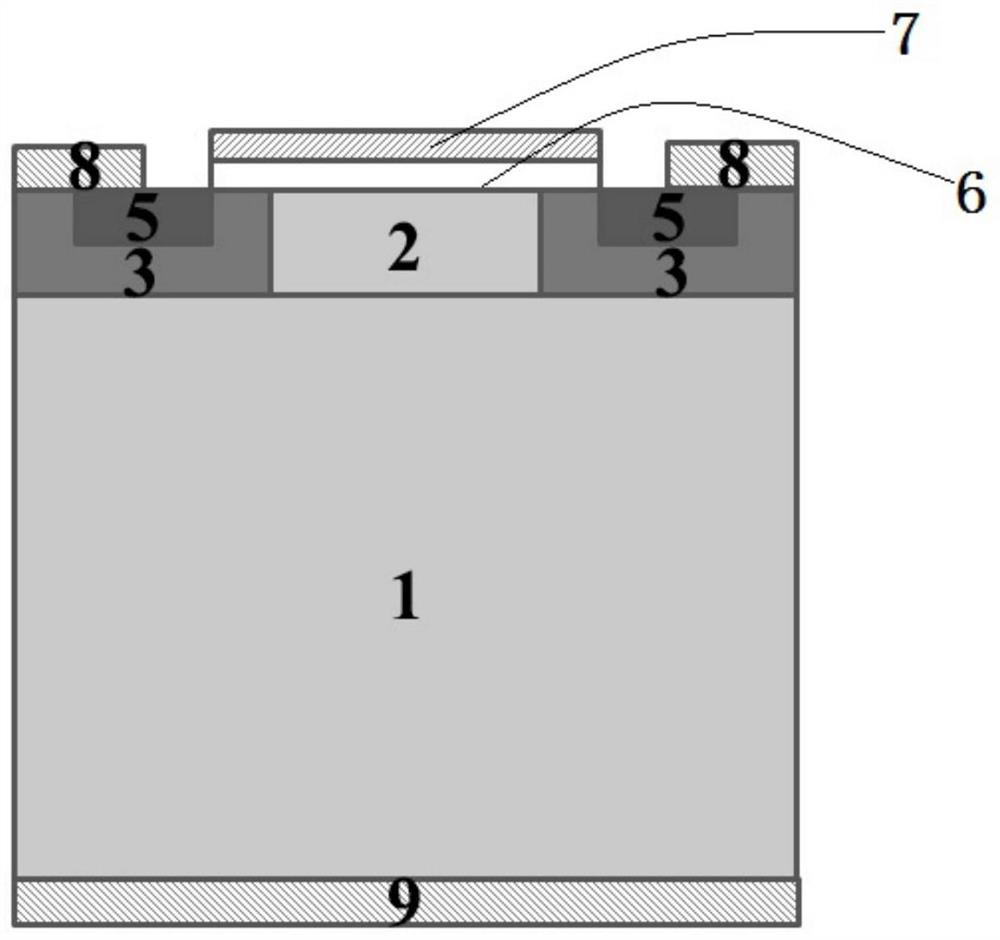
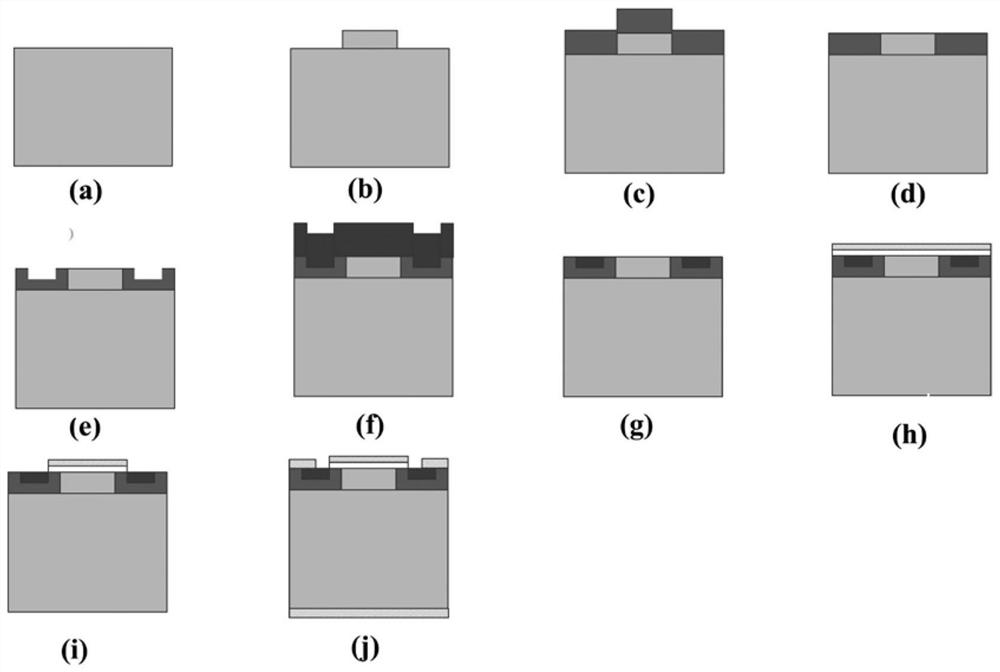
[0019] Embodiment 1: as image 3 Shown is the process of manufacturing MOSFET devices.

[0020] (1) Epitaxially grow the epitaxial layer 1 so as to meet the blocking requirements of the device, such as image 3 as shown in (a);

[0021] (2) Mesa 2 is etched on the epitaxial layer, such as image 3 as shown in (b);

[0022] (3) Epitaxially growing the initial well region 3 on the mesa, the height of the initial well region should be greater than or equal to the height of the mesa; as image 3 as shown in (c);

[0023] (4) Use the CMP process to obtain a well area with a flat and smooth surface, and the height of the well area obtained after the CMP process is the same as the height of the mesa, such as image 3 as shown in (d);

[0024] (5) Obtain the groove area 4 by using processes such as etching, such as image 3 as shown in (e);

[0025] (6) The thickness of the initial source region 5 for epitaxial growth is higher than the depth of the groove region 4, and the he...

example 2

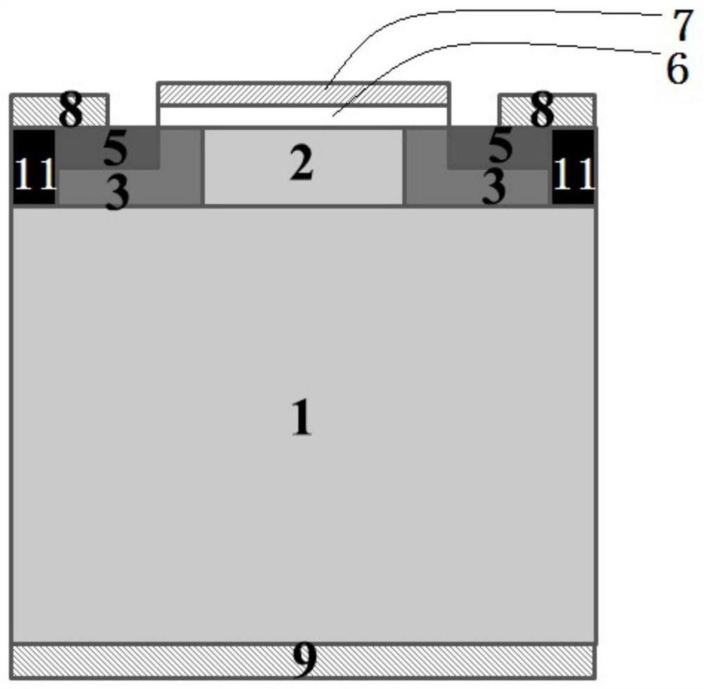
[0031] Example 2: if Figure 4 Shown is the process of manufacturing IGBT devices.

[0032] (1) Epitaxially grow the epitaxial layer 1 so as to meet the blocking requirements of the device, such as Figure 4 as shown in (a);

[0033] (2) The mesa 2 etched on the epitaxial layer, such as Figure 4 as shown in (b);

[0034] (3) The initial well region 3 is epitaxially grown on the mesa, and the height of the initial well region is greater than or equal to the height of the mesa, such as Figure 4 as shown in (c);

[0035] (4) Use the CMP process to obtain a flat and smooth well region, and the height of the obtained well region is the same as the height of the mesa, such as Figure 4 as shown in (d);

[0036] (5) Obtain the groove area 4 by using processes such as etching, such as Figure 4 as shown in (e);

[0037] (6) The thickness of the initial source region 5 for epitaxial growth is higher than the depth of the groove region, and the height of the initial source reg...


PUM


Abstract

The invention discloses an MOS type device and a manufacturing method thereof. The MOS device comprises an epitaxial layer, a mesa above the epitaxial layer, and a well region which is arranged abovethe epitaxial layer and distributed at both sides of the mesa, wherein the well region is etched to acquire a trench region, a source region is acquired through epitaxial grow in the acquired trench region, a gate oxide layer and a gate electrode sequentially grow above the mesa, a source electrode is arranged above the well region, and a drain electrode is arranged below the epitaxial layer. TheMOS device is advantaged in that the well region and the source region are formed through the epitaxial process and the CMP process, the ion implantation process for preparing the well region and thesource region is not needed, crystal lattice damage caused by ion implantation can be reduced, doping concentration of the well region and the source region can be accurately controlled, and thereby length of channels is not restricted by photolithography accuracy.

Description

technical field [0001] The invention relates to a power semiconductor and its manufacturing method, in particular to a MOS type device and its manufacturing method. Background technique [0002] The MOS type device structure has the advantages of simple gate control circuit, short turn-on time and short turn-off time, which makes the MOS type device greatly beneficial to the integration of circuits. The well region and source region of MOS devices are usually completed by processes such as ion implantation. Ion implantation requires enormous energy and can cause damage to the crystal lattice of the material. Although it can be repaired to a certain extent by processes such as high temperature annealing, it will leave permanent lattice damage. In addition, the requirements of the ion implantation process are relatively high. Contents of the invention [0003] Purpose of the invention: In order to solve the damage to the material lattice caused by ion implantation to form...

Claims


Application Information

Patent Timeline
Patent Type & Authority Patents(China)
IPC IPC(8): H01L29/78H01L21/336H01L29/80
CPCH01L29/66227H01L29/78H01L29/80
Inventor 杨同同柏松黄润华
Owner NO 55 INST CHINA ELECTRONIC SCI & TECHNOLOGYGROUP CO LTD
Why Eureka
Try Eureka