


Quick Research
Generate reliable direction feasibility study reports for your R&D in just a few steps.

Technical Q&A
Discover and master advanced knowledge NOW. Basics, ideas, possibilities, all at once.

Find Solutions
As an expert in R&D theories, this can generate solutions to your technical problems instantly.

Evaluate Feasibility
Analyze your overall solution with one click, know your potential R&D risks in advance.

Monitor Landscape
Get weekly tech updates, stay abreast of the latest tech innovations and key insights.
Method for preparing amorphous silicon by ALD
An amorphous silicon, reaction source technology, applied in the direction of final product manufacturing, sustainable manufacturing/processing, semiconductor/solid-state device manufacturing, etc., can solve the problems of high production cost, complex process flow, etc., achieve simple production, increase window , suitable for thinning effect
- Summary
- Abstract
- Description
- Claims
- Application Information
AI Technical Summary
Problems solved by technology
Method used
Image

Examples
Embodiment 1
[0022] A method for making amorphous silicon by ALD, comprising the following steps:
[0023] (1) Open the furnace door of the ALD (atomic layer deposition) equipment, put the sample made of amorphous silicon into the carrier, and vacuumize the equipment;
[0024] (2) The leakage rate of the equipment test is ≤5mTorr / min, and the temperature is raised to 200°C and kept at a constant temperature for 10 minutes;
[0025] (3) Feed the reaction source trimethylsilane and nitrogen, and grow amorphous silicon several times in this way according to the growth thickness, and the feeding amount of trimethylsilane and nitrogen is determined according to the actual situation;
[0026] (4) Pass N 2 Purge the special gas pipeline and pass N at the same time 2 Return the furnace tube to normal pressure;
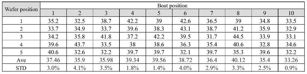
[0027] (5) The sample of the furnace door is opened.
[0028] Table 1 Example 1 prepared amorphous silicon thickness and uniformity results
[0029]
Embodiment 2
[0031] A method for making amorphous silicon by ALD, comprising the following steps:
[0032] (1) Open the furnace door of the ALD (atomic layer deposition) equipment, put the sample made of amorphous silicon into the carrier, and vacuumize the equipment;
[0033] (2) Equipment test leakage rate = 3mTorr, while raising the temperature to 300°C and keeping the temperature constant for 15min;
[0034] (3) Feed the reaction source dichlorodiethylsilane and nitrogen, and grow amorphous silicon in this way several times according to the growth thickness;
[0035] (4) Pass N 2 Purge the special gas pipeline and pass N at the same time 2 Return the furnace tube to normal pressure;
[0036] (5) The sample of the furnace door is opened.
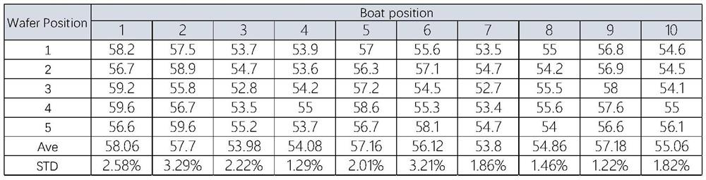
[0037] Table 2 The thickness and uniformity results of the amorphous silicon prepared in Example 2
[0038]
Embodiment 3
[0040] A method for making amorphous silicon by ALD, comprising the following steps:
[0041] (1) Open the furnace door of the ALD (atomic layer deposition) equipment, put the sample made of amorphous silicon into the carrier, and vacuumize the equipment;
[0042] (2) Equipment test leakage rate = 2mTorr, while raising the temperature to 500°C and keeping the temperature constant for 5min;
[0043] (3) Feed in the reaction source disilane and nitrogen, and grow amorphous silicon several times in this way according to the growth thickness;
[0044] (4) Pass N 2 Purge the special gas pipeline and pass N at the same time 2 Return the furnace tube to normal pressure;
[0045] (5) The sample of the furnace door is opened.
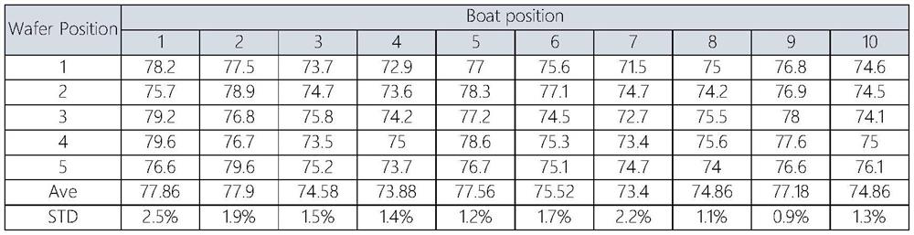
[0046] The amorphous silicon thickness and uniformity result that table 3 embodiment 3 prepares
[0047]
PUM
 Abstract
Description
Claims
Application Information
 - R&D Engineer
- R&D Manager
- IP Professional
- Industry Leading Data Capabilities
- Powerful AI technology
- Patent DNA Extraction
Browse by: Latest US Patents, China's latest patents, Technical Efficacy Thesaurus, Application Domain, Technology Topic, Popular Technical Reports.
© 2024 PatSnap. All rights reserved.Legal|Privacy policy|Modern Slavery Act Transparency Statement|Sitemap|About US| Contact US: help@patsnap.com