
Quantum authentication system integrated on single circuit board

An authentication system and circuit board technology, applied in the fields of quantum security authentication, identity recognition, and quantum encryption, can solve the problems of extremely high requirements on position alignment and stability, inflexible and convenient use, and bulky, so as to avoid position alignment. problem, compact structure, small size effect

Active Publication Date: 2017-05-31
INST OF ELECTRONICS ENG CHINA ACAD OF ENG PHYSICS
View PDF7 Cites 12 Cited by
  • Summary
  • Abstract
  • Description
  • Claims
  • Application Information

AI Technical Summary

Benefits of technology

This patented technology describes how it can be used for securely transmitting digital data over wireless communication networks without compromising its security or privacy level. It combines two technologies: Optically Unclonable Function (OUI) with Physically Random Access Memory (RAM). These combined features make them more efficient than traditional methods like encryption techniques that require physical contact from users' devices. Overall, this new method provides greater safety measures against unauthorized access while still being effective at encrypting sensitive data transmissions effectively.

Problems solved by technology

The technical problem addressed in this patented text relates to developing an efficient way to verify user's privacy through digital signatures without compromising their integrity during these processes. Current methods involve complicated optically designed devices like QKENS® and other specialty hardware platforms, but they require expensive equipment and may still result in significant loss if hacking attempts take place at any time. This patents proposes a solution involving integrating quantum autologous functions into existing infrastructure while reducing complexity and improving ease of operation.

Method used


Image

  • Quantum authentication system integrated on single circuit board
  • Quantum authentication system integrated on single circuit board
  • Quantum authentication system integrated on single circuit board

Examples


Embodiment Construction

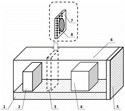
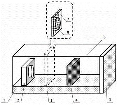
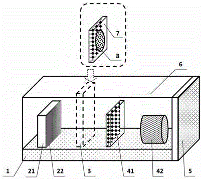
[0032] Such as figure 1 As shown, a quantum authentication system integrated on a single circuit board includes: an integrated circuit board 1, a quantum light source module 2, a card slot, a decoding detection module 4, a touch screen display chip 5, and a blackened inner surface shell 6 , the excitation light modulator chip 7 and the optical PUF 8; the quantum light source module 2, the card slot 3, and the decoding detection module 4 are integrated on the integrated circuit board 1 sequentially from left to right through soldering, and the card slot 3 is inserted Connected to the excitation light modulator chip 7, the touch screen display chip 5 is welded to the rightmost end of the integrated circuit board 1, and the integrated circuit board 1 and the touch screen display chip 5 are used as two end faces to be packaged into one through the shell 6. The touch screen display chip The display interface of 5 is exposed outside the whole; the optical PUF8 package is fixed on th...


PUM


Abstract

The invention discloses a quantum authentication system integrated on a single circuit board. The quantum authentication system comprises an integrated circuit board, a quantum light source module, a card slot, a decoding detection module, a touch screen display chip and a quantum key card formed by an incentive optical modulator chip with a window on which an optical PUF is fixedly packaged, wherein the quantum light source module, the card slot, the decoding detection module and the touch screen display chip are sequentially interconnected and integrated on the integrated circuit board through soldering from left to right and are integrally packaged through a shell. According to the quantum authentication system integrated on the single circuit board, the optical PUF and the incentive optical modulator chip are integrated, and the purpose of position alignment between excitation light and the optical PUF is achieved; the purpose of position alignment between the quantum key card and the decoding detection module is achieved through the wave-front feedback adaptive algorithm, and the stability and the repeatability of the system are greatly improved. The quantum authentication system integrated on the single circuit board also has the advantages of being small in size, light in weight, compact in structure and fast and convenient to use and carry, and is suitable for the fields of quantum security certification, identity recognition and quantum encryption.

Description


Claims


Application Information

Patent Timeline
Owner INST OF ELECTRONICS ENG CHINA ACAD OF ENG PHYSICS
Learn More