Improved groove-type Schottky rectifier device and manufacturing method thereof
A rectifier device and manufacturing method technology, applied in the direction of semiconductor devices, electrical components, circuits, etc., can solve the problems of large forward conduction voltage drop, etc., and achieve low pinch-off voltage, large contact area between metal and semiconductor, and pinch-off speed fast effect
- Summary
- Abstract
- Description
- Claims
- Application Information
AI Technical Summary
Problems solved by technology
Method used
Image
Examples
no. 1 example
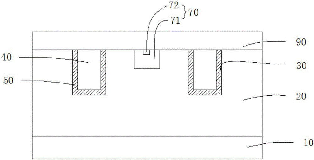
[0032] Such as figure 1 As shown, the improved trench Schottky rectifier device of this embodiment includes: a first conductivity type substrate 10, a first conductivity type conduction layer 20 formed on the first conductivity type substrate 10, formed The trench 30 in the upper surface layer of the first conductivity type conduction layer 20, the conductive polysilicon 40 filling the trench 30, and the gate insulating layer 50 formed between the trench 30 and the conductive polysilicon 40, The metal electrode layer 60 formed on the surface of the first conductivity type conduction layer 20, the second conductivity type region 70 is provided in the upper surface layer of the first conductivity type conduction layer 20 between two adjacent grooves 30, the The metal electrode layer 60 is disposed on the first conductivity type conduction layer 20 , the conductive polysilicon 40 and the second conductivity type region 70 .
[0033] In this embodiment, the first conductivity typ...
no. 2 example
[0047] Such as figure 2 As shown, the trench type Schottky rectifier device of this embodiment is basically the same as the technical solution of the first embodiment, the difference is that the doping concentration of the second conductivity type region 70 in this embodiment is higher than that of the first conductivity type. The enhanced region 90 of the first conductivity type of the conduction layer 20, the enhanced region 90 of the first conductivity type is formed directly under the region 70 of the second conductivity type, and does not affect the lateral depletion of the PN junction and the MOS structure to pinch off the Schottky barrier region. In this case, that is, without affecting the reverse withstand voltage capability, the carrier concentration of the conductive layer is increased, and the forward conduction voltage drop is reduced.
[0048] Preferably, the enhancement region 90 of the first conductivity type is not in contact with the second conductivity type...
PUM
 Abstract
Description
Claims
Application Information
 - R&D
- Intellectual Property
- Life Sciences
- Materials
- Tech Scout
- Unparalleled Data Quality
- Higher Quality Content
- 60% Fewer Hallucinations
Browse by: Latest US Patents, China's latest patents, Technical Efficacy Thesaurus, Application Domain, Technology Topic, Popular Technical Reports.
© 2025 PatSnap. All rights reserved.Legal|Privacy policy|Modern Slavery Act Transparency Statement|Sitemap|About US| Contact US: help@patsnap.com


