Optical processing systems and methods

A technology of optical processing and optical path direction, applied in optics, opto-mechanical equipment, microlithography exposure equipment, etc., can solve the problems of difficulty in obtaining stripe outline, influence of pattern outline, unbearable, etc., to achieve clear pattern outline and better equipment performance. Excellent, fast response and reliable effect

Active Publication Date: 2018-12-14
ADVANCED TERAHERTZ SYST (SUZHOU) CO LTD
View PDF10 Cites 0 Cited by
  • Summary
  • Abstract
  • Description
  • Claims
  • Application Information

AI Technical Summary

Problems solved by technology

[0006] 1. System performance is limited by SLM materials
Under the current technical conditions, various phase modulation devices including LCoS can only use liquid crystal materials, the refresh frequency is low (about 100Hz) and cannot withstand large optical power, which is not conducive to the realization of efficient photolithography processing
In addition, the liquid crystal material has low transmittance to ultraviolet light and will be damaged, so its lithography system cannot use short-wavelength light sources, which is not conducive to obtaining high-resolution lithography patterns
[0007] 2. It is difficult to obtain a clear fringe outline
It can be seen from the reference that the outline of its lithographic pattern is still not clear enough, especially when the stripe period is large
[0008] The master's thesis "Continuously Variable Space-Frequency Interferometric Lithography Technology for Diffractive Spatial Imaging" proposed another interference lithography system and method based on spatial light modulator. The focal plane, the exposure plane is located on the rear focal plane of the lens, which does not satisfy the imaging relationship, so in principle it is impossible to achieve a clear graphic outline output
Patent CN201210440974.2 "A System and Method for Interferometric Lithography Based on Spatial Light Modulator" also has the same problem. In addition, the spectrum plane needs to be filtered, which further affects the graphic profile
[0009] Based on the above analysis, the existing interference lithography technology cannot achieve high-quality and high-efficiency interference pattern processing

Method used


Image

  • Optical processing systems and methods
  • Optical processing systems and methods
  • Optical processing systems and methods

Examples


Embodiment 1

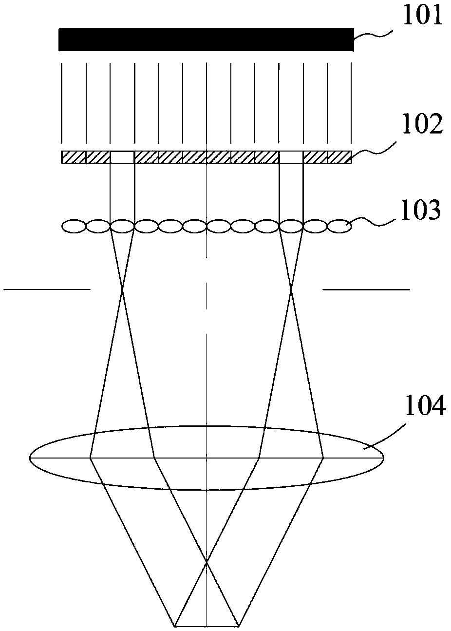
[0061] combine Figure 4 As shown, a front-stage mirror group is also provided in the direction of the optical path, and the front-stage mirror group is arranged between the spatial light modulator 102 and the microlens array 103. The front-stage mirror group includes a first lens 201 and a second lens arranged along the direction of the optical path. Two lenses 202 .

[0062] In this technical solution, the front-stage mirror group is a projection imaging optical path, which is composed of a first lens and a second lens. It has two functions: 1. The front-stage lens group projects the SLM into the front focal plane of the microlens array 103 . The precise matching of the unit size and the overall format of the SLM and the microlens array 103 can be realized through optical zooming. 2. The focal length of the microlens array 103 is very short (about a few millimeters), and the space between the optical path elements is narrow, making adjustment difficult. After adopting the...

Embodiment 2

[0074] combine Figure 5As shown, on the basis of the first embodiment, this embodiment also includes a seventh lens 301 and a switching device. In the first state, the switching device drives the front-stage lens group and the microlens array 103 as a whole 302 to move to the spatial light modulator 102 and the optical path between the imaging lens (group) 104, in the second state, the switching device drives the seventh lens 301 to move to the optical path between the spatial light modulator 102 and the imaging lens (group) 104, and simultaneously the front-stage lens group and microlens array 103 as a whole 302 out.

[0075] In this technical solution, this solution can realize the sharing of interference lithography and imaging lithography, so that one device has two functions, and can realize the precise registration of interference lithography images and imaging lithography, in printing and packaging, security It has important applications in identification and micro-na...


PUM

PropertyMeasurementUnit
wavelengthaaaaaaaaaa

Abstract

The invention discloses an optical processing system and an optical processing method. The system comprises a lighting source, a spatial light modulator, a micro-lens array and an imaging lens (group) sequentially arranged along the light path direction, wherein the spatial light modulator is positioned on the front focal plane of the micro-lens array; the front focal plane of the imaging lens (group) is overlapped with the rear focal plane of the micro-lens array; the spatial light modulator is of an amplitude type and has multiple blocks in two-dimensional distribution; the micro-lens array comprises multiple micro-lenses distributed in the same plane; each micro-lens is corresponding to a block in the primary optical axis direction. The system and method disclosed by the invention at least have the advantages of no mechanical movement mechanism, fast and reliable response, better equipment performance, clear graph outline and acquisition of multiple interference figures.

Description

technical field [0001] The present application belongs to the field of laser processing, and in particular relates to an optical processing system and method. Background technique [0002] Photolithography is the main method for the preparation of micro-nano structures. The current lithography technology is mainly divided into two categories: imaging lithography and interference lithography. Imaging lithography is suitable for the production of arbitrary graphic structures, while interference lithography is more suitable for the production of specific periodic structures. These periodic structures are usually formed by the interference and superposition of two or more beams on the exposure surface. The typical pattern There are parallel stripes (that is, gratings), orthogonal dot matrix and hexagonal patterns, etc. Based on the directional deflection characteristics of periodic structures to light fields, interference lithography is widely used in digital holography and thr...

Claims


Application Information

Patent Timeline
Patent Type & Authority Patents(China)
IPC IPC(8): G03F7/20
CPCG03F7/70291G03F7/70358G03F7/70408G03F7/70466
Inventor 李继刚
Owner ADVANCED TERAHERTZ SYST (SUZHOU) CO LTD
Why Eureka
Try Eureka