
Loading method capable of controlling buffering type multilayer polycrystalline silicon seed crystal melting

A polysilicon and buffer layer technology, which is applied in the growth of polycrystalline materials, chemical instruments and methods, and crystal growth, can solve problems such as uneven silicon material composition, seed crystal layer melting through, and seed crystal layer overmelting, etc., to reduce Effects of defect clusters, reduction of grain boundary formation, and high product yield

Inactive Publication Date: 2017-05-31
NANTONG UNIVERSITY
View PDF11 Cites 1 Cited by
  • Summary
  • Abstract
  • Description
  • Claims
  • Application Information

AI Technical Summary

Problems solved by technology

However, due to the different sizes of silicon materials and the uneven composition of silicon materials, there must be some places that melt quickly and some places that melt slowly.
When the fast-melting area reaches the seed layer, it starts to melt the seed layer, and the slow-melting area has not touched the seed layer. Generally speaking, the thickness of the seed layer is only 15-20mm. Therefore, if there is an area If the melting is particularly fast, it will inevitably cause over-melting or even melting through of the seed layer in this area. If the uneven distribution of melting temperature is considered, the melting of some areas will be faster, and it is easier to cause the melting of the seed layer

Method used


Image

  • Loading method capable of controlling buffering type multilayer polycrystalline silicon seed crystal melting
  • Loading method capable of controlling buffering type multilayer polycrystalline silicon seed crystal melting
  • Loading method capable of controlling buffering type multilayer polycrystalline silicon seed crystal melting

Examples


specific Embodiment

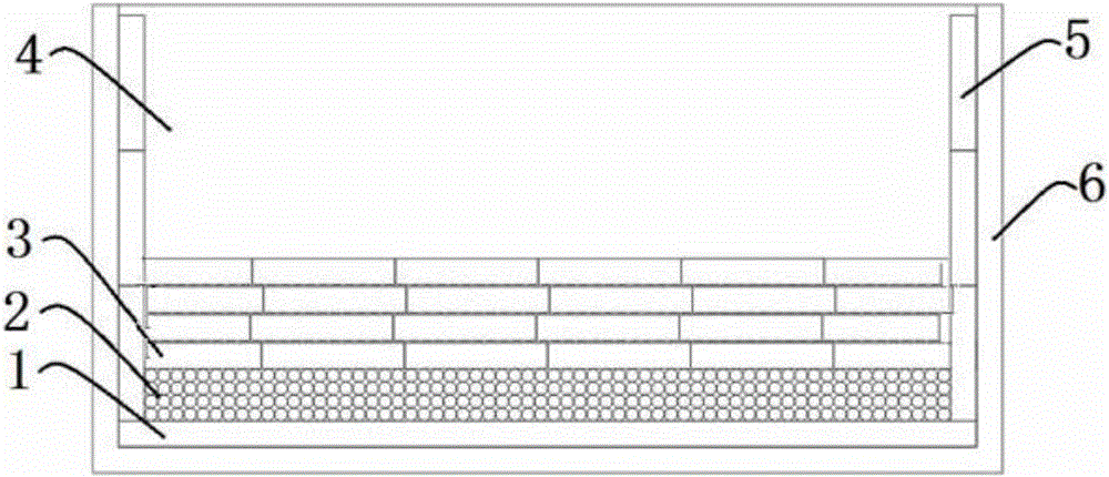
[0023] refer to figure 1 Shown, a kind of charging method of buffer type multi-layer polysilicon seed melting control, comprises the following steps:

[0024] Step a, laying a layer of polysilicon block on the bottom of the crucible 6 as the seed crystal layer 1 of the directional solidification semi-melting process, and the thickness of the seed crystal layer 1 is 12-18mm;

[0025] Step b, stacking small particles of primary polysilicon material and fine polysilicon fragments on the seed layer 1 as a buffer layer 2, the filling height of the buffer layer 2 is 100-150mm;

[0026] Step c, stacking multi-layer polysilicon bricks on the buffer layer 2 as the barrier layer 3, the length, width and height of the polysilicon bricks are 156 mm, 156 mm, and 30-40 mm respectively, and the center of the barrier layer 3 A total of 25 crystal bricks are used at the place, and each side is filled with crystal bricks; the inner wall of the crucible 6 is provided with polysilicon crystal br...


PUM

PropertyMeasurementUnit
Thicknessaaaaaaaaaa

Abstract

The present invention discloses a loading method capable of controlling buffering type multilayer polycrystalline silicon seed crystal melting. The method comprises following steps: paving a layer of polycrystalline silicon blocks as a seed crystal layer in an orient coagulation-casting semi-melting technology; stacking up small granule type raw polycrystalline silicon materials and fine polycrystalline silicon fragments on the seed crystal layer to be used as a buffering layer; stacking up multilayers of polycrystalline silicon crystal bricks on the buffering layer to be used as a blocking layer; fully filling gaps of the polycrystalline silicon crystal bricks with the small granule type raw polycrystalline silicon materials; and stacking up following materials on the blocking layer in sequence: seed materials, the raw polycrystalline silicon materials, head and tail materials and edge materials until stacked materials are higher than a crucible by 100-120mm. In the method, by combined application of blocking layer and buffering layer, a straight solid-liquid interface can be obtained, silicon ingots can grow easily in an outside extending manner, crystal grains are relatively even, columnar crystals are relatively complete, the formation of defect clusters and crystal grain boundaries is reduced, and the quality of the silicon ingots is improved.

Description

technical field [0001] The invention belongs to the field of polysilicon melting, and relates to a charging method for controlling the melting of buffered multi-layer polysilicon seed crystals. Background technique [0002] Melting is a very important stage in the ingot casting process. The speed and uniformity of silicon material melting are very important for the semi-melting process. Generally speaking, since the heater of the ingot furnace is located on the top and side walls of the ingot furnace, the melting of the silicon material in the furnace mainly starts from the top and then gradually melts down. Under the action of gravity, the molten silicon liquid will permeate downward, and gradually melt the silicon material on the path during the permeation process, and finally achieve the purpose of complete melting. However, due to the different sizes of the silicon material and the uneven composition of the silicon material, there must be some places that melt quickly a...

Claims


Application Information

Patent Timeline
IPC IPC(8): C30B29/06C30B28/06
CPCC30B29/06C30B28/06
Inventor 邓洁尤敏王强朱海峰邓洪海章国安
Owner NANTONG UNIVERSITY
Learn More