Multi-stage magnetic field electric-arc ion plating method for lining positive-bias step-shaped pipe
An arc ion plating and positive bias technology, applied in the field of material surface treatment, can solve the problems of low arc plasma transmission efficiency and large particle defects, avoid large particle defects, improve crystal structure and stress state, and improve transmission efficiency. Effect
- Summary
- Abstract
- Description
- Claims
- Application Information
AI Technical Summary
Problems solved by technology
Method used
Image
Examples
specific Embodiment approach 1
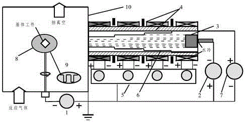
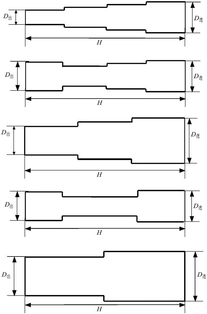
[0015] Specific implementation mode one: the following combination figure 1 and 2 Describe the present embodiment, the device used in the multistage magnetic field arc ion plating method of lining positive bias stepped pipe in this embodiment includes a bias power supply 1, an arc power supply 2, an arc ion plating target source 3, a multistage magnetic field device 4, Multi-stage magnetic field power supply 5, lined positive bias stepped tube device 6, positive bias power supply 7, sample stage 8, bias power supply waveform oscilloscope 9 and vacuum chamber 10;
[0016] The method includes the following steps:
[0017] Step 1. Place the substrate workpiece to be processed on the sample stage 8 in the vacuum chamber 10, and insulate the liner positive bias stepped tube device 6 from the vacuum chamber 10 and the multi-stage magnetic field device 4, and connect the workpiece to the sample stage 8. The negative output end of the bias power supply 1, the arc ion plating target ...
specific Embodiment approach 2
[0026] Embodiment 2: The difference between this embodiment and Embodiment 1 is that the method also includes:
[0027] Step 3: Thin films can be deposited by combining traditional DC magnetron sputtering, pulsed magnetron sputtering, traditional arc ion plating and pulsed cathodic arc with DC bias, pulse bias or DC pulse composite bias to prepare pure metal films , compound ceramic films with different element ratios, functional films and high-quality films with nano-multilayer or gradient structures.
specific Embodiment approach 3
[0028] Embodiment 3: The difference between this embodiment and Embodiment 2 is that Steps 1 to 3 are repeated to prepare multi-layered thin films with different stress states, microstructures and element ratios, and the others are the same as Embodiment 2.
PUM
 Abstract
Description
Claims
Application Information
 - Generate Ideas
- Intellectual Property
- Life Sciences
- Materials
- Tech Scout
- Unparalleled Data Quality
- Higher Quality Content
- 60% Fewer Hallucinations
Browse by: Latest US Patents, China's latest patents, Technical Efficacy Thesaurus, Application Domain, Technology Topic, Popular Technical Reports.
© 2025 PatSnap. All rights reserved.Legal|Privacy policy|Modern Slavery Act Transparency Statement|Sitemap|About US| Contact US: help@patsnap.com


