Epitaxial wafer of green light emitting diode and growth method thereof
A technology of a light-emitting diode and a growth method, which is applied to the epitaxial wafer of a green light-emitting diode and its growth field, can solve the problems of large lattice mismatch, low luminous efficiency, inability of a P-type electron blocking layer to effectively suppress electron overflow, and the like, To achieve the effect of improving lattice mismatch, improving luminous efficiency, and facilitating electron overflow
- Summary
- Abstract
- Description
- Claims
- Application Information
AI Technical Summary
Problems solved by technology
Method used
Image


Examples
Embodiment 1
[0035] An embodiment of the present invention provides an epitaxial wafer of a green light emitting diode, see figure 1 , the epitaxial wafer includes a sapphire substrate 1, and a buffer layer 2, an undoped GaN layer 3, an N-type layer 4, a multi-quantum well layer 5, a P-type electron blocking layer 6, P-type layer 7 and P-type contact layer 8 .
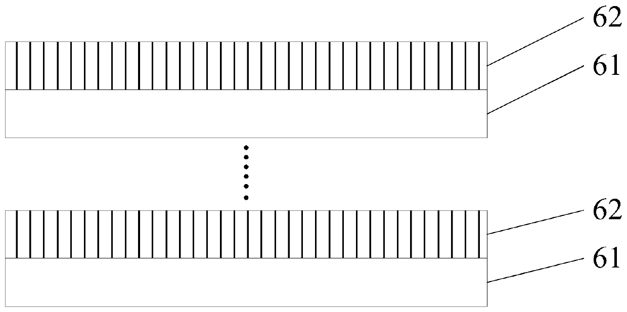
[0036] In this example, see figure 2 , the P-type electron blocking layer 6 includes several sublayers stacked in sequence, and the sublayers include In x al 1-x N layer 61 and stacked on In x al 1-x In on N layer 61 y al z Ga 1-y-z N layer 62, 0<x<1, 0<y<1, 0<z<1.
[0037] Optionally, the thickness of the P-type electron blocking layer may be less than 100 nm, so as not to hinder hole injection into the multiple quantum well layer.
[0038] Optionally, In x al 1-x The thickness of the N layer can be 1-20nm, In y al z Ga 1-y-z The thickness of the N layer can be 1-20 nm, so as to avoid adverse effects on the lattice ...
Embodiment 2
[0065] An embodiment of the present invention provides a method for growing an epitaxial wafer of a green light-emitting diode, which is suitable for growing the epitaxial wafer provided in Embodiment 1, see Figure 4 , the growth method includes:
[0066] Step 201: Provide a sapphire substrate.
[0067] Step 202: growing a buffer layer, an undoped GaN layer, an N-type layer, a multi-quantum well layer, a P-type electron blocking layer, a P-type layer and a P-type contact layer sequentially on the sapphire substrate.
[0068] In this embodiment, the P-type electron blocking layer includes several sequentially stacked sublayers, and the sublayers include In x al 1-x N layers and stacked on In x al 1-x In on N layer y al z Ga 1-y-z N layers, 0<x<1, 0<y<1, 0<z<1.
[0069] Specifically, the buffer layer can be a GaN layer, the N-type layer can be a Si-doped GaN layer, the multi-quantum well layer can include alternately stacked InGaN quantum well layers and GaN quantum bar...
Embodiment 3
[0099] The embodiment of the present invention provides a method for growing an epitaxial wafer of a green light-emitting diode, which is a concrete realization of the growth method provided in Embodiment 2, and is realized with high-purity hydrogen (H 2 ) or nitrogen (N 2 ) as carrier gas, trimethylgallium (TMGa), trimethylaluminum (TMAl), trimethylindium (TMIn) and ammonia (NH 3 ) as Ga, Al, In and N sources respectively, with silane (SiH 4 ), Magnesium (Cp 2 Mg) as N and P type dopants respectively.
[0100] Specifically, see Figure 5 , the growth method includes:
[0101] Step 301: The temperature of the substrate is first raised to 500°C, then raised to 800°C and stabilized for 30s, then raised to 1000°C and stabilized for 30s, then raised to 1230°C and stabilized for 10 minutes, and then heat-treated in a pure hydrogen atmosphere.
[0102] It should be noted that the purpose of heat treatment is to clean the substrate surface.
[0103] Step 302: Lower the temperat...
PUM
 Abstract
Description
Claims
Application Information
 - R&D
- Intellectual Property
- Life Sciences
- Materials
- Tech Scout
- Unparalleled Data Quality
- Higher Quality Content
- 60% Fewer Hallucinations
Browse by: Latest US Patents, China's latest patents, Technical Efficacy Thesaurus, Application Domain, Technology Topic, Popular Technical Reports.
© 2025 PatSnap. All rights reserved.Legal|Privacy policy|Modern Slavery Act Transparency Statement|Sitemap|About US| Contact US: help@patsnap.com