Method for producing indium phosphide back hole

A manufacturing method and technology of indium phosphide, which are applied in semiconductor/solid-state device manufacturing, semiconductor/solid-state device components, semiconductor devices, etc., can solve the problems of InP back-hole fabrication and other problems, and achieve good consistency and repeatability. Simple process, simple and controllable effect

Active Publication Date: 2017-05-17
NO 55 INST CHINA ELECTRONIC SCI & TECHNOLOGYGROUP CO LTD
View PDF11 Cites 5 Cited by
  • Summary
  • Abstract
  • Description
  • Claims
  • Application Information

AI Technical Summary

Problems solved by technology

[0004] High-temperature etching has certain requirements for a series of related backside processes, such as the bonding separation mechanism and the selection of etchi

Method used


Image

  • Method for producing indium phosphide back hole
  • Method for producing indium phosphide back hole
  • Method for producing indium phosphide back hole

Examples


Embodiment

[0033] The method for making an indium phosphide back hole includes the following steps:

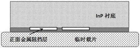
[0034] (1) Make a layer of 300nm TiPtAu metal barrier layer on the front of the indium phosphide wafer. After the front process is completed, stick the front of the indium phosphide wafer to the sapphire with high-temperature wax, and then use a grinder to grind the indium phosphide substrate The thickness is reduced to 100um;

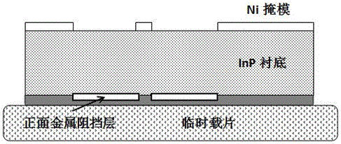
[0035] (2) Use photoresist to lithography the back hole pattern, and then evaporate Ni metal as an etching mask;

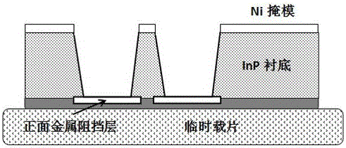
[0036] (3) Use the back helium of the STS ICP dry etching machine to raise the temperature of the wafer to 190 degrees, and use chlorine gas (Cl 2 ) and argon (Ar) to etch indium phosphide at an etching rate of about 1um / min;

[0037] (4) Remove the Ni etching mask with dilute hydrochloric acid;

[0038] (5) Sputter the seed layer Ti / Au / Ti on the back of the indium phosphide wafer, and then electroplate about 5um of Au, so that the bottom of the b...


PUM


Abstract

The invention provides a method for producing an indium phosphide back hole. The method comprises the following steps: step (1), producing a metal barrier layer at a position of the front of a indium phosphide wafer where the back hole needs to be configured, and finishing a front process; step (2), bonding the front of the wafer to a temporary slide sapphire, and thinning and polishing the back of the wafer; step (3), photoetching a back hole figure at the back of the wafer, ensuring that the back hole position is consistent with the front metal barrier layer, and forming an etching mask; step (4), rising the back helium temperature of an STS ICP dry etching machine to 190 DEG C, using the combined gas of chlorine (C12) and argon Ar to perform dry etching, until etching to the front metal barrier layer; step (5), removing the etching mask; and step (6), sputtering a seed layer at the back, electroplating a back gold and filling the back hole, and then finishing the back hole production. The method for producing the indium phosphide back hole provided by the invention has the following advantages that the problem of etching an indium phosphide deep hole has been solved; the back hole morphology, the etching repeatability and the coherence are all very good; and meanwhile, the process is simple and can be compatible with the GaAs process, thus the method is suitable for large-scale popularization and application.

Description

technical field [0001] The invention relates to a method for manufacturing an indium phosphide back hole, which belongs to the technical field of semiconductor integrated circuits. Background technique [0002] Indium phosphide (InP) devices have superior characteristics such as ultra-high speed and low power consumption, and have great potential in the manufacture of high-speed millimeter-wave monolithic integrated circuits (MMICs) and submillimeter-wave monolithic integrated circuits (SMMICs). They are broadband As a key component of wireless communication systems and terahertz imaging systems, it has attracted widespread attention. The back hole is a key process of MMIC manufacturing. By thinning the wafer substrate and opening the substrate to form a ground via, it can effectively reduce the parasitic inductance and ground resistance, and can better dissipate heat. After the introduction of backholes, people have manufactured high-performance GaAs circuits, forming a re...

Claims


Application Information

Patent Timeline
IPC IPC(8): H01L23/482H01L21/60
CPCH01L24/19H01L24/24H01L2224/24105H01L2224/2413H01L2224/19
Inventor 常龙程伟王元
Owner NO 55 INST CHINA ELECTRONIC SCI & TECHNOLOGYGROUP CO LTD
Why Eureka
Try Eureka