N-type bi-directional HEMT device based on CH3NH3PbI3 material and preparation method thereof

A device and N-type technology, applied in the field of N-type bidirectional HEMT devices and their preparation, can solve the problems of inability to meet the needs of photoelectric high electron mobility transistors, and achieve the effects of high photoelectric conversion efficiency, enhanced device performance, and high mobility

Active Publication Date: 2017-05-10
XIDIAN UNIV
View PDF3 Cites 3 Cited by
  • Summary
  • Abstract
  • Description
  • Claims
  • Application Information

AI Technical Summary

Problems solved by technology

[0004] Traditional inorganic HEMT high electron mobility transistors belong to the conversion of electric energy to electric energy, and cannot meet the demand for optoelectronic high electron mobility transistors in the visible light band.

Method used


Image

  • N-type bi-directional HEMT device based on CH3NH3PbI3 material and preparation method thereof
  • N-type bi-directional HEMT device based on CH3NH3PbI3 material and preparation method thereof
  • N-type bi-directional HEMT device based on CH3NH3PbI3 material and preparation method thereof

Examples


Embodiment 1

[0050] Traditional HEMT high electron mobility transistors are complex and costly, while CH-based 3 NH 3 PB 3 The preparation of the material HEMT is simple and the cost is low; the traditional inorganic HEMT high electron mobility transistor belongs to the conversion of electric energy to electric energy, which cannot meet the demand for optoelectronic high electron mobility transistors in the visible light band, and the CH 3 NH 3 PB 3 The material has both the properties of organic / inorganic materials and its own excellent optoelectronic properties, which can well meet the market demand for optoelectronic high electron mobility transistors in the visible light band. Based on CH 3 NH 3 PB 3 The HEMT of the material can generate a large number of photogenerated carriers through light to realize the conversion of electric energy plus light energy to electric energy, and improve the conversion efficiency. In addition, based on CH 3 NH 3 PB 3 The HEMT of the material can...

Embodiment 2

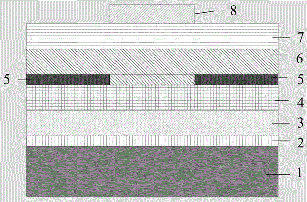
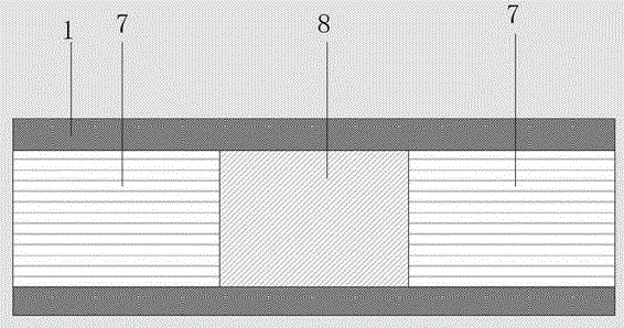
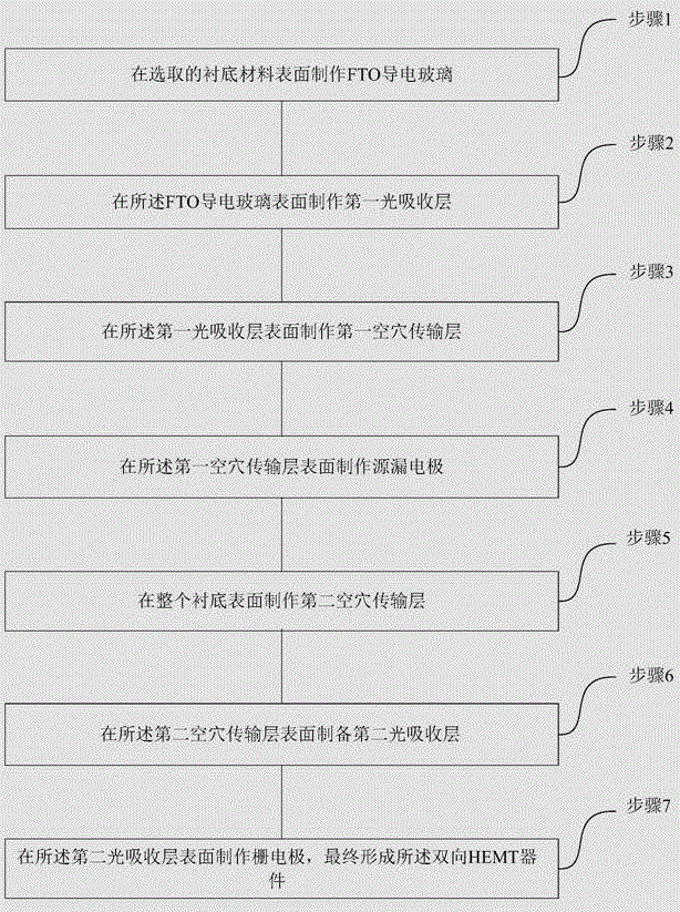
[0084] Please also see Figure 4a-Figure 4h and Figure 5 and Figure 6 , Figure 4a-Figure 4h A schematic diagram of a preparation method for an N-type bidirectional HEMT device based on a CH3NH3PbI3 material provided by an embodiment of the present invention; Figure 5 A schematic structural diagram of a first mask plate provided by an embodiment of the present invention; Figure 6 A schematic structural diagram of a second mask plate provided by an embodiment of the present invention. In this embodiment, on the basis of the above-mentioned embodiments, the CH-based 3 NH 3 PB 3 The preparation method of the N-type bidirectional HEMT device of the material is described in detail as follows:

[0085] Step 1: See Figure 4a, to prepare sapphire Al 2 o 3 The substrate 1 has a thickness of 200 μm-600 μm.

[0086] The substrate is sapphire Al 2 o 3 Reason: Due to its low price and good insulation performance, it can effectively prevent the longitudinal leakage of bidi...


PUM

PropertyMeasurementUnit
Thicknessaaaaaaaaaa
Thicknessaaaaaaaaaa
Thicknessaaaaaaaaaa

Abstract

The invention relates to an N-type bi-directional HEMT device based on a CH3NH3PbI3 material and a preparation method thereof. The method comprises the steps that a substrate is selected; an FTO film is formed; the CH3NH3PbI3 material is prepared to form a first light absorbing layer; a first electron transport layer is formed on the surface of the first light absorbing layer; source and drain electrodes are formed on the surface of the first electron transport layer; a second electron transport layer is formed on the surface of the first electron transport layer which is not covered by source and drain electrodes and source and drain electrodes; the CH3NH3PbI3 material is prepared on the surface of the second electron transport layer to form a second light absorbing layer; and a gate electrode is formed on the surface of the second light absorbing layer to finally form the bi-directional HEMT device. According to the invention, the symmetrical light absorbing layers are used to absorb more light to generate photogenerated carriers; transparent conductive glass grows on transparent sapphire as the bottom gate electrode, so that upper and lower light can irradiate the light absorbing layers; the CH3NH3PbI3 provides a large number of electrons for the channel; the mobility is improved; and the transmission characteristic and the photoelectric conversion efficiency are improved.

Description

technical field [0001] The invention belongs to the technical field of integrated circuits, in particular to a CH-based 3 NH 3 PB 3 The N-type bidirectional HEMT device of the material and its preparation method. Background technique [0002] With the vigorous development of electronic technology, semiconductor integrated circuits play an increasingly important role in social development and national economy. Among them, the market demand for optoelectronic high-speed devices is increasing day by day, and higher and more detailed requirements are constantly put forward for the performance of the devices. In order to seek a breakthrough, no matter from the aspects of technology, material or structure, the research has been uninterrupted. In recent years, with the rise of visible light wireless communication technology and circuit coupling technology, the market has put forward new requirements for optoelectronic High Electron Mobility Transistor (HEMT) tubes in the visibl...

Claims


Application Information

Patent Timeline
IPC IPC(8): H01L51/05H01L51/30H01L51/40
CPCH10K85/30H10K10/46
Inventor 贾仁需刘银涛汪钰成庞体强张玉明
Owner XIDIAN UNIV
Why Eureka
Try Eureka