
Novel anti-radiation device structure

A device structure and anti-radiation technology, which is applied in semiconductor devices, electrical components, circuits, etc., can solve the problems of carrier mobility reduction, device performance degradation, and affecting gate control ability, so as to improve the anti-radiation ability, Reduce device performance degradation, reduce the effect of device performance degradation

Inactive Publication Date: 2017-05-03
UNIV OF ELECTRONICS SCI & TECH OF CHINA
View PDF0 Cites 7 Cited by
  • Summary
  • Abstract
  • Description
  • Claims
  • Application Information

AI Technical Summary

Problems solved by technology

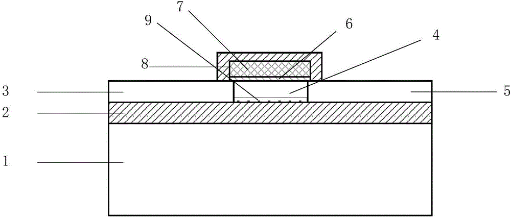
[0005] Under irradiation conditions, oxide trap charges are introduced into the 2-insulating buried oxide layer, such as image 3 As shown, these trapped charges will attract electrons in the silicon layer to form a parasitic conductive channel, which will increase the leakage current of the device; at the same time, due to the influence of coupling, this part of the trapped charges will affect the control ability of the gate and degrade the performance of the device
At the same time, SiO with low thermal conductivity in SOI structure 2 layer will cause the heat generated by the channel current to be unable to dissipate in time, the internal temperature of the device is too high, the carrier mobility is reduced, and the output current of the device is reduced

Method used


Image

  • Novel anti-radiation device structure
  • Novel anti-radiation device structure
  • Novel anti-radiation device structure

Examples


Embodiment Construction

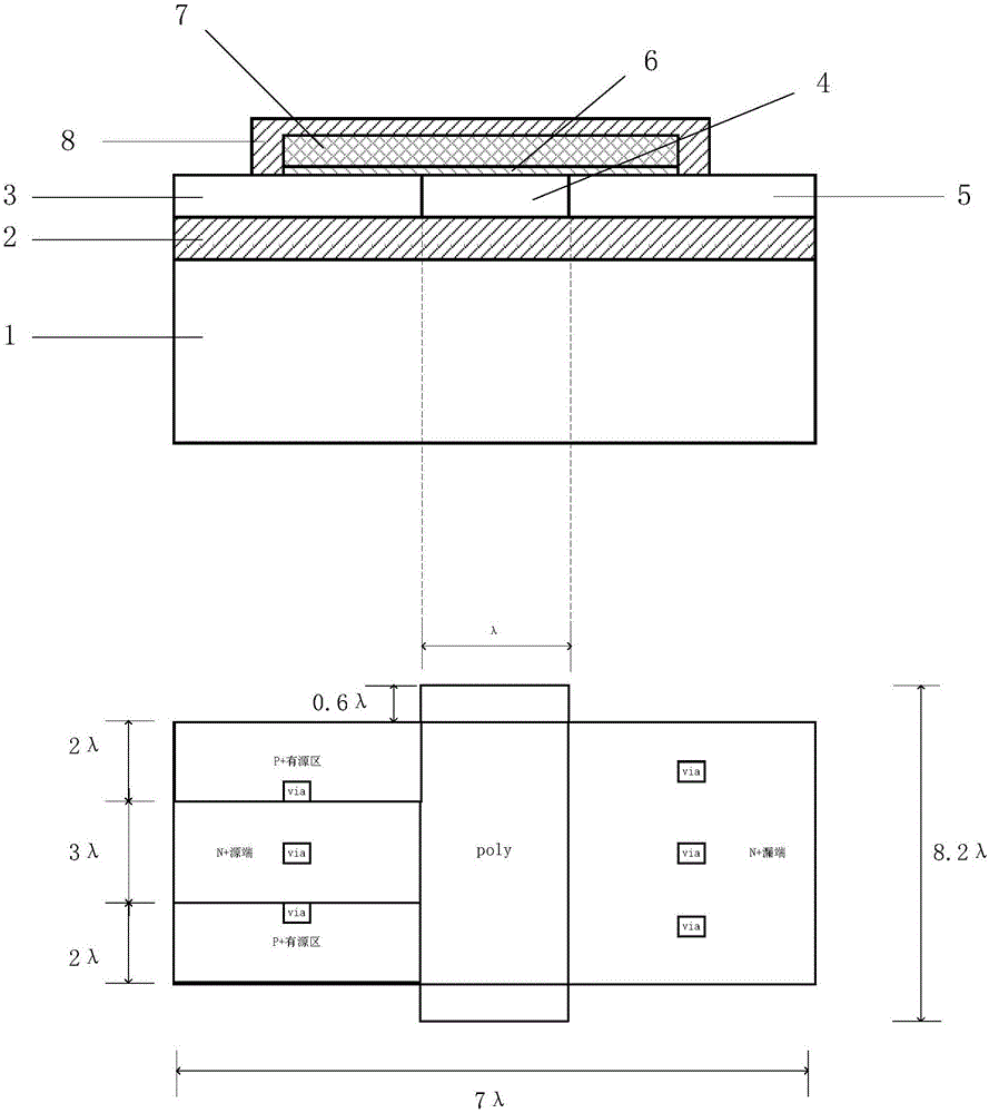
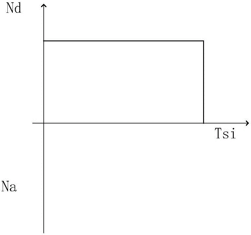
[0020] Such as Figure 6 Shown: and figure 1 Compared with the SOI device of the conventional structure shown in , the thicker SiO2 in the conventional SOI device 2 The insulating buried layer is replaced by an ultra-thin buried oxide layer obtained by low-dose, low-energy oxygen ion implantation, due to the reduction of SiO 2 The thickness of the layer can effectively reduce the self-heating effect. Moreover, using the above method, the thickness of the top silicon film obtained is smaller, it is easier to form a fully depleted device, and it is less affected by the body effect. In the case of single-event radiation, the charge accumulated on the top silicon film is less. At the same time thinner SiO 2 The buried layer can release excess carriers into the substrate through the tunneling effect, further reducing the conductivity of the back channel controlled by the back gate. Such as Figure 4 As shown, using low-dose, low-energy oxygen ion implantation, the obtained SOI...


PUM


Abstract

The invention belongs to the technical field of anti-radiation semiconductors, and relates to an SOI device capable of improving anti-radiation performance of the device based on a mainstream semiconductor process condition. The anti-radiation SOI device related by the invention is characterized in that through changing an insulating buried layer, the self-heating effect of the SOI device is reduced; and meanwhile, charges accumulated on a surface of a back gate can be reduced under a radiation condition; through changing a doped structure of an active area, a leakage current produced by a parasitic channel under the radiation condition is reduced, and simultaneously the body contact is realized better; and through changing a BTS structure, under the condition of keeping unchanged length-to-width ratio of the channel and the effective body contact, the layout area can be reduced. A novel anti-radiation device structure, under the condition of being compatible to a mainstream SOI process, can have the characteristics of relatively small self-heating effect, relatively small leakage current and relatively small layout area, etc.

Description

technical field [0001] The invention relates to the field of integrated circuits and space technology, in particular to an SOI device based on mainstream semiconductor process conditions and capable of improving the radiation resistance performance of the device. Background technique [0002] Under irradiation conditions, integrated circuits and electronic components will produce various radiation effects such as total dose, single particle, and instantaneous radiation. If the devices and circuits used in artificial earth satellites, space probes, and manned spacecraft do not undergo special anti-radiation hardening measures, their performance will soon degrade and become invalid, causing huge safety hazards and cost waste. Therefore, it is of great significance for the development of space technology to actively seek methods for devices and circuits with high resistance to radiation energy. [0003] Due to the use of full dielectric isolation, SOI devices have obvious diff...

Claims


Application Information

Patent Timeline
Patent Type & Authority Applications(China)
IPC IPC(8): H01L29/06H01L29/08H01L29/78
CPCH01L29/78H01L29/0649H01L29/0847
Inventor 李平刘洋
Owner UNIV OF ELECTRONICS SCI & TECH OF CHINA
Learn More