
Patsnap Eureka
For R&D, Patsnap Eureka makes reading and utilizing patents & technical documents easy.
Patsnap Eureka AIR
Designed for self-driven R&D workflows. Generate viable solutions, solve complex R&D challenges, empower your innovation with AI.

Patsnap Eureka Materials
Designed for material experts only. Revolutionize your material R&D, from search, analyze, to developing new materials.

TechResearch
Generate reliable direction feasibility study reports for your R&D in just a few steps.

TechSeek
Discover and master advanced knowledge NOW. Basics, ideas, possibilities, all at once.

TechMind
As an expert in R&D Theories, TechMind can generates customized viable solutions instantly.

TechRisk
Analyze your overall solution with one click, know your potential R&D risks in advance.

TechMonitor
Get weekly tech updates, stay abreast of the latest tech innovations and key insights.
Gan thin film grown on glass substrate and preparation method thereof
A glass substrate and thin film technology, applied in semiconductor devices, electrical components, circuits, etc., can solve the problems of high LED manufacturing cost, high price, expensive sapphire and SiC substrates, etc., to reduce production costs, easy to obtain, The effect of improving photoelectric conversion efficiency
- Summary
- Abstract
- Description
- Claims
- Application Information
AI Technical Summary
Problems solved by technology
Method used
Image

Examples
Embodiment 1
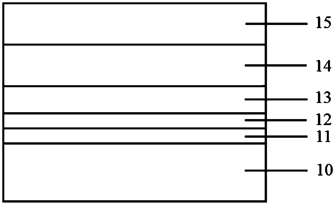
[0039] Such as figure 1 As shown, the GaN thin film grown on the glass substrate of the present embodiment includes an aluminum metal layer 11 grown on the glass substrate 10, a silver metal layer 12 grown on the aluminum metal layer, and a silver metal layer grown on the silver metal layer 12 AlN buffer layer 13, a GaN buffer layer 14 grown on the AlN buffer layer 13, and a GaN thin film 15 grown on the GaN buffer layer 14.
[0040] The preparation method of the GaN thin film grown on the glass substrate of the present embodiment comprises the following steps:
[0041] (1) Selection of substrate: use ordinary glass substrate;
[0042] (2) Substrate surface polishing and cleaning treatment;
[0043] The surface polishing of the substrate is specifically:
[0044] First, the surface of the glass substrate is polished with diamond slurry, and the surface of the substrate is observed with an optical microscope until there are no scratches, and then the chemical mechanical poli...
Embodiment 2
[0057] The preparation method of the GaN thin film grown on the glass substrate of the present embodiment comprises the following steps:
[0058] (1) Selection of substrate: use ordinary glass substrate;
[0059] (2) Substrate surface polishing and cleaning treatment;
[0060] The surface polishing of the substrate is specifically:
[0061] First, the surface of the glass substrate is polished with diamond slurry, and the surface of the substrate is observed with an optical microscope until there are no scratches, and then the chemical mechanical polishing method is used for polishing;
[0062] The cleaning is specifically:
[0063] Put the glass substrate into deionized water and ultrasonically clean it at room temperature for 5 minutes to remove the dirt particles on the surface of the glass substrate, then wash it with acetone and ethanol in sequence to remove the surface organic matter, and dry it with high-purity dry nitrogen;
[0064] (3) Growth of the aluminum metal ...
PUM
| Property | Measurement | Unit |
|---|---|---|
| thickness | aaaaa | aaaaa |
| thickness | aaaaa | aaaaa |
| thickness | aaaaa | aaaaa |
Abstract
Description
Claims
Application Information
 - R&D Engineer
- R&D Manager
- IP Professional
- Industry Leading Data Capabilities
- Powerful AI technology
- Patent DNA Extraction
Browse by: Latest US Patents, China's latest patents, Technical Efficacy Thesaurus, Application Domain, Technology Topic, Popular Technical Reports.
© 2024 PatSnap. All rights reserved.Legal|Privacy policy|Modern Slavery Act Transparency Statement|Sitemap|About US| Contact US: help@patsnap.com