Ultraviolet LED epitaxial structure with novel quantum barrier structure and preparation method thereof
A technology of epitaxial structure and quantum barrier, which is applied in the direction of electrical components, circuits, semiconductor devices, etc., can solve the problems of low internal quantum efficiency and low luminous efficiency, so as to slow down the polarization effect, improve the radiation recombination efficiency, and improve the internal quantum efficiency Effect
- Summary
- Abstract
- Description
- Claims
- Application Information
AI Technical Summary
Problems solved by technology
Method used
Image
Examples
Embodiment 1
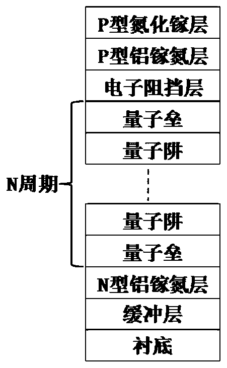
[0028] The first embodiment of the present invention provides an ultraviolet LED epitaxial structure with a novel quantum barrier structure, such as figure 1 As shown, the ultraviolet LED epitaxial wafer includes from bottom to top: substrate, buffer layer, N-type aluminum gallium nitride layer, light emitting layer, electron blocking layer, P-type aluminum gallium nitride layer and P-type gallium nitride layer, preferably , the N-type AlGaN layer is Al a Ga 1-a N, where 0n Ga 1-n N, wherein the value range of the aluminum component n is y<n<1.
[0029] The light-emitting layer includes at least 3 periods of quantum barrier layers and quantum well layers, and the quantum well layers are Al b Ga 1- b N, wherein the value range of aluminum component b is 0≤b figure 2 As shown, each quantum barrier includes Al from bottom to top x Ga 1-x N layer, Al y Ga 1-y N layer and Al z Ga 1-z N layer; except the first and last quantum barriers from the bottom up in the light-emit...
Embodiment 2
[0034] The second embodiment of the present invention provides a method for preparing an ultraviolet LED epitaxial structure with a novel quantum barrier structure, comprising the following steps:
[0035] The substrate is a C-plane sapphire substrate; the sapphire substrate is placed in a metal organic compound chemical vapor deposition epitaxial reaction chamber, a hydrogen environment is set at a temperature of 1280° C., and the substrate is baked for 5 minutes;
[0036] The buffer layer is grown on the substrate, the growth temperature of the buffer layer is 1200° C., and the growth thickness is 2.5-3 μm.
[0037] The N-type AlGaN layer is grown on the buffer layer, the growth temperature of the N-type AlGaN layer is controlled at 1200° C., the thickness of the N-type AlGaN layer is controlled at 3 μm, and the N-type doping concentration is 2 ×10 18 ㎝ -3 .
[0038] A nitrogen environment is set at a temperature of 1000-1200° C., and a luminescent layer is grown on the N...
PUM
 Abstract
Description
Claims
Application Information
 - R&D
- Intellectual Property
- Life Sciences
- Materials
- Tech Scout
- Unparalleled Data Quality
- Higher Quality Content
- 60% Fewer Hallucinations
Browse by: Latest US Patents, China's latest patents, Technical Efficacy Thesaurus, Application Domain, Technology Topic, Popular Technical Reports.
© 2025 PatSnap. All rights reserved.Legal|Privacy policy|Modern Slavery Act Transparency Statement|Sitemap|About US| Contact US: help@patsnap.com


