
A low-defect mutation buffer layer with chirped digitally graded structure

A buffer layer, low-defect technology, applied in electrical components, circuits, semiconductor devices, etc., can solve problems such as insignificant effects, and achieve the effects of improving crystal quality, reducing residual strain and defect density, and simplifying the growth process.

Active Publication Date: 2018-03-09
无锡中科德芯感知科技有限公司
View PDF4 Cites 0 Cited by
  • Summary
  • Abstract
  • Description
  • Claims
  • Application Information

AI Technical Summary

Problems solved by technology

Although the insertion of the superlattice is expected to partially block defect transmission, the effect is not obvious from the reported results of actual devices

Method used


Image

  • A low-defect mutation buffer layer with chirped digitally graded structure
  • A low-defect mutation buffer layer with chirped digitally graded structure
  • A low-defect mutation buffer layer with chirped digitally graded structure

Examples


Embodiment 1

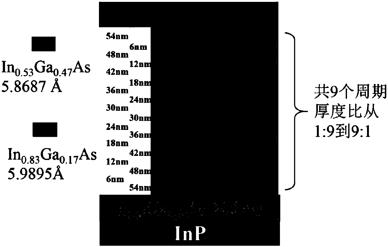
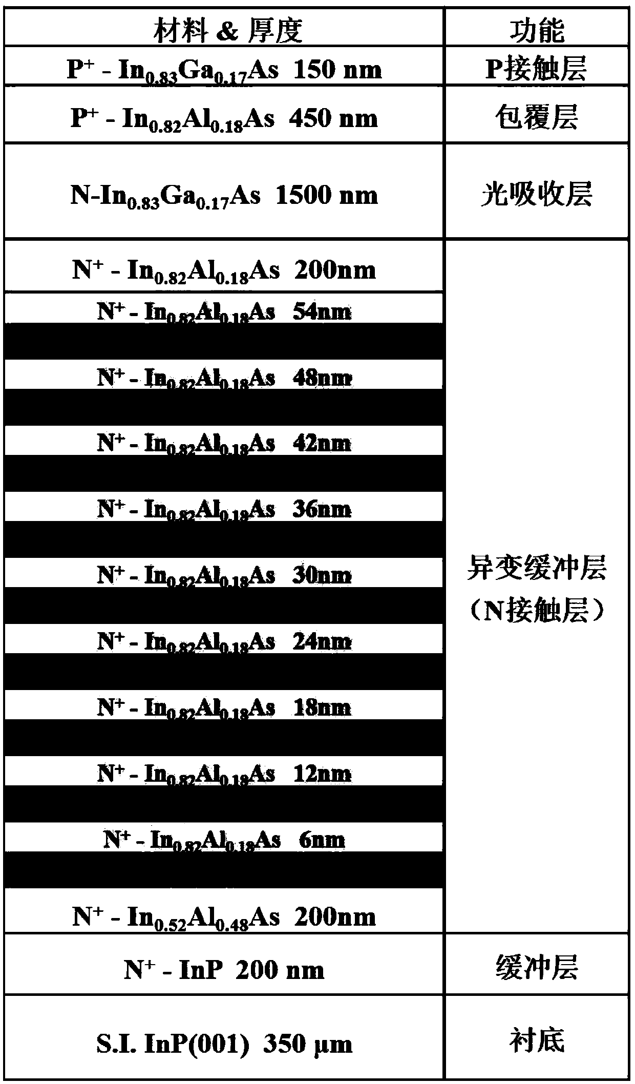
[0034] The purpose of this example is to epitaxially grow lattice-mismatched In on an InP substrate. 0.83 Ga 0.17 As the light-absorbing layer, the preparation of the detector material with the photoresponse cut-off wavelength at room temperature of 2.6 μm is realized. Since In 0.83 Ga 0.17 There is a lattice mismatch between As and the InP substrate, so the chirped digital gradient variation buffer layer growth technique was used to prepare In with an In composition of 0.82 0.82 Al 0.12 As virtual substrate, and on the basis of this virtual substrate, epitaxially grow PIN type photodiode device structure. The specific device structure is as image 3 shown. Its structure contains the following materials in order from bottom to top:

[0035] 1. Semi-insulating (S.I.) InP (001) substrate. Thickness 350μm, resistivity ρ≥1MΩ·cm.

[0036] 2. N-type heavy doping (N + ) InP buffer layer. Thickness 200nm, doping concentration 4×10 18 cm -3 .

[0037] 3. N-type heavy dopi...


PUM


Abstract

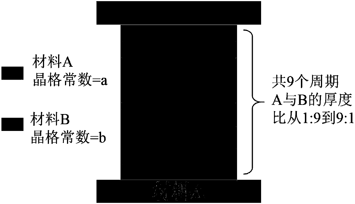
The invention relates to a low defect metamorphic buffer layer of a chirp digital-graded structure. The buffer layer includes N periodic transition layers which have same thickness. Each period includes two layers of materials, an A layer and a B layer, and the A layer and B layer are graded from a thickness ratio of N:1 to 1:N. According to the invention, the buffer layer by using the blockage effects on dislocation defect transmission imposed by chirp digital-graded periodic interface, realizes noticeable reduction in defect density near the surface of the metamorphic buffer layer, has noticeable increase in the quality of a material crystal, and can simultaneously achieve crystal lattice and energy band double transition. The buffer layer is expected to be widely applied to the increase of properties of heterostructure mismatch lasers and probes on substrates, such as Si, GaAs, InP, and GaSb.

Description

technical field [0001] The invention belongs to the field of semiconductor materials, in particular to a low-defect variation buffer layer with a chirped digital gradient structure. Background technique [0002] Semiconductor heterogeneous epitaxial growth technology was developed in the late 1950s and early 1960s. It is a material preparation technology for obtaining high-quality semiconductor single crystals developed along with the development of semiconductor vacuum epitaxy equipment. It refers to the process of growing a semiconductor single crystal thin film different from the substrate material on a semiconductor single crystal substrate according to the crystal orientation of the substrate. The material, conductivity type, and resistivity of the single crystal layer grown by heteroepitaxy can be different from the substrate, and multilayer heterogeneous single crystal materials with different thicknesses and different requirements can be grown, thus greatly improving...

Claims


Application Information

Patent Timeline
Patent Type & Authority Patents(China)
IPC IPC(8): H01L31/0352H01L21/02
CPCH01L21/02392H01L21/02463H01L21/02507H01L21/02546H01L31/035263
Inventor 马英杰顾溢张永刚
Owner 无锡中科德芯感知科技有限公司
Learn More