A kind of semiconductor device and its preparation method, electronic device
A semiconductor and device technology, applied in the field of semiconductor devices and their preparation, can solve the problems of device performance degradation and weak Si-O
- Summary
- Abstract
- Description
- Claims
- Application Information
AI Technical Summary
Problems solved by technology
Method used
Image

Examples
Embodiment 1
[0043]In order to solve the problems in the prior art, the present invention provides a new method for manufacturing a semiconductor device. The method of the present invention will be further described below in conjunction with the accompanying drawings.
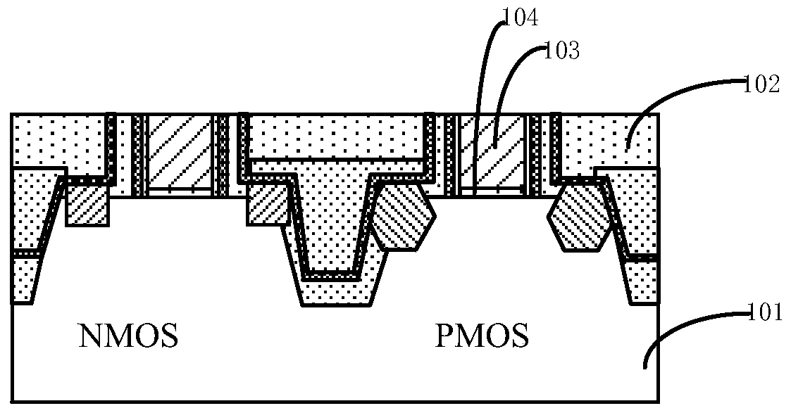
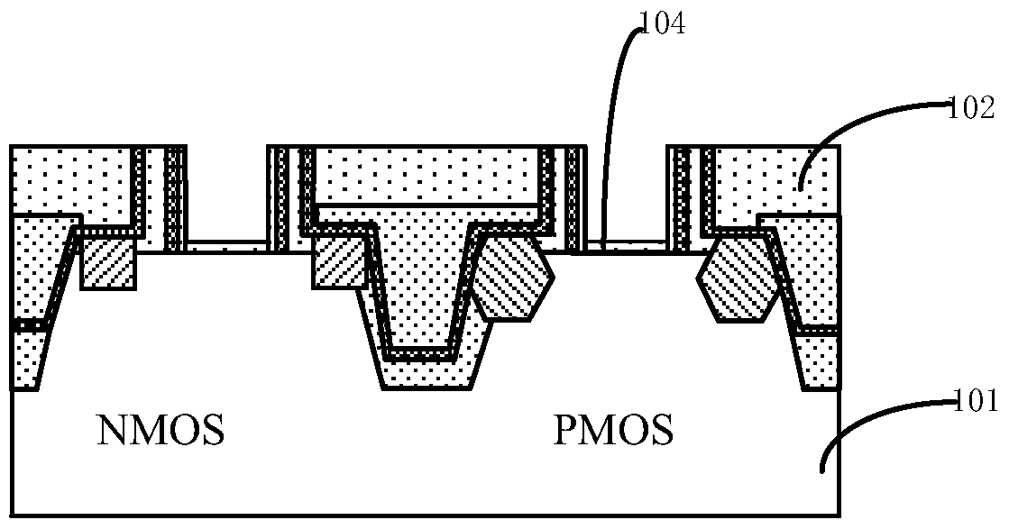
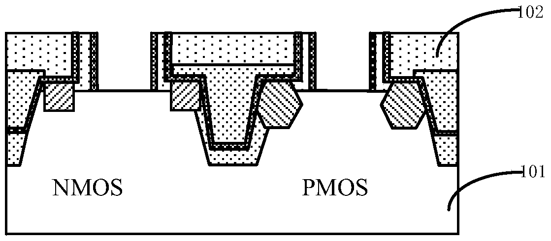
[0044] in, Figures 1a-1n It is a schematic diagram of the manufacturing process of the semiconductor device described in a specific implementation of the present invention.
[0045] First, step 101 is performed to provide a semiconductor substrate on which several fins and a dummy gate oxide layer surrounding the fins and a dummy gate are formed, and a plurality of fins are formed on the semiconductor substrate. There is an interlayer dielectric layer filling gaps between adjacent dummy gates.
[0046] Specifically, the method includes the following steps:
[0047] Step 1011: providing a semiconductor substrate 101 and performing ion implantation to form wells.
[0048] Specifically, such as Figure 1a As shown, in this...
Embodiment 2
[0128] The present invention also provides a semiconductor device, which is prepared by the method described in the first embodiment.
[0129] The semiconductor device includes a semiconductor substrate 101, and the semiconductor substrate may be at least one of the materials mentioned below: silicon, silicon-on-insulator (SOI), silicon-on-insulator (SSOI), germanium-on-insulator Silicon (S-SiGeOI), silicon germanium on insulator (SiGeOI) and germanium on insulator (GeOI), etc. In this embodiment, silicon is selected as the semiconductor substrate 101 .
[0130] Wherein the semiconductor substrate includes an NMOS region and a PMOS region, so as to form NMOS devices and PMOS devices in subsequent steps.
[0131] A plurality of fins are formed on the semiconductor substrate, and the fins all have the same width, or the fins are divided into a plurality of fin groups having different widths.
[0132] The semiconductor device further includes a metal gate structure disposed aro...
Embodiment 3
[0144] The present invention also provides an electronic device, including the semiconductor device described in the second embodiment. Wherein, the semiconductor device is the semiconductor device described in the second embodiment, or the semiconductor device obtained according to the preparation method described in the first embodiment.
[0145] The electronic device of this embodiment can be any electronic product or equipment such as mobile phone, tablet computer, notebook computer, netbook, game console, TV set, VCD, DVD, navigator, camera, video recorder, voice recorder, MP3, MP4, PSP, etc. , can also be any intermediate product including the semiconductor device. The electronic device according to the embodiment of the present invention has better performance due to the use of the above-mentioned semiconductor device.
PUM
 Abstract
Description
Claims
Application Information
 - R&D
- Intellectual Property
- Life Sciences
- Materials
- Tech Scout
- Unparalleled Data Quality
- Higher Quality Content
- 60% Fewer Hallucinations
Browse by: Latest US Patents, China's latest patents, Technical Efficacy Thesaurus, Application Domain, Technology Topic, Popular Technical Reports.
© 2025 PatSnap. All rights reserved.Legal|Privacy policy|Modern Slavery Act Transparency Statement|Sitemap|About US| Contact US: help@patsnap.com