Charge-trapping type storage element and preparation technology therefor

A storage element and charge trapping technology, applied in electrical components, electric solid-state devices, circuits, etc., can solve problems such as difficult to meet memory performance requirements, low storage density, high power consumption, etc., achieve good stability and retention characteristics, low power consumption, the effect of simple structure

Active Publication Date: 2017-04-12
HEBEI UNIVERSITY
View PDF2 Cites 6 Cited by
  • Summary
  • Abstract
  • Description
  • Claims
  • Application Information

AI Technical Summary

Problems solved by technology

[0004] Applications. ACS Appl. Mater. Interfaces 2011, 3, 4619−4625.), Oruc uses HfO 2 The memory window prepared as a trapping layer was 1.6 V at an operating voltage of ±5 V (Oruc, F. B.; Cimen, F.; Rizk, A.; Ghaffari, M.; Nayfeh, A.; Okyay, A. K. Thin -Film ZnO Charge-Trapping Memory Cell Grown in a Single ALD Step. IEEE Electron Device Lett. 2012, 33, 1714−1716.), these have the problems of high power consumption and low storage density
[0005] Due to the arrival of the 32nm process node, these existing charge-trapping memories are difficult to meet people's future performance requirements for lower power consumption and higher storage density memories

Method used


Image

  • Charge-trapping type storage element and preparation technology therefor
  • Charge-trapping type storage element and preparation technology therefor
  • Charge-trapping type storage element and preparation technology therefor

Examples


Embodiment 1

[0035] (1) Selection and treatment of substrate material: P-type Si (100) was selected as the substrate, and it was cleaned in acetone, alcohol, and deionized water by ultrasonic waves for 10 minutes respectively, and set aside.

[0036] (2) if Figure 6 As shown, in the magnetron sputtering film forming system, the sputtering material target 4 (Ga 2 o 3 The target material) is fixed on the target stage 5 of the magnetron sputtering film-making system, and the substrate material 1 (that is, the P-type Si (100) substrate cleaned and prepared in step (1)) is fixed on the substrate stage 2, Then all are placed in the growth chamber 6.

[0037] (3) Use a vacuum pump to evacuate the growth chamber 6 to 2.0×10 through the interface valve 7 of the mechanical pump and the molecular pump. -4 Pa; then pass the mixed gas of 25 sccm of argon and 25 sccm of oxygen from the charging valve 8 through the external gas circuit system; then start the radio frequency transmitter 9, adjust the in...

Embodiment 2-4

[0048] The annealing temperature was changed (see Table 1 for details), and other conditions were the same as in Example 1.

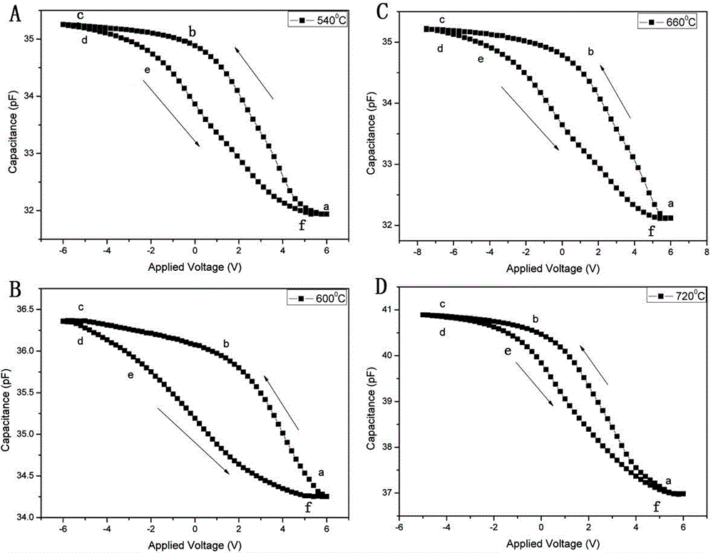
[0049] The element voltage-capacitance relationship characteristic prepared by embodiment 2-4 is detected, and the results are as follows: image 3 In A, C, and D, the statistical results of the size of the storage window are shown in Table 1.

[0050] In addition, the TEM scanning method was used to detect the generated SiO 2 The thickness of the tunneling layer, the results are shown in Table 1.

[0051] Table 1:

[0052]

[0053] Depend on image 3 , Figure 4 It can be seen from the statistical results in Table 1 that the storage element of the present invention is ideal as a whole in the annealing temperature range of 540-720°C, but as the annealing temperature increases, the SiO 2 The thickness of the tunneling layer also increases gradually. When the annealing temperature is 600°C, the thickness of the tunneling layer of the storage eleme...

Embodiment 5-12

[0055] Change Ga 2 o 3 Layer thickness and annealing temperature (see Table 2 for details), and other conditions are the same as in Example 1.

[0056] Table 2:

[0057]

[0058] It can be seen from the statistical results in Table 2 that Ga 2 o 3 The storage element made by layer thickness in the range of 35-65nm is generally ideal, but the Ga 2 o 3 When the layer thickness is about 50nm, the storage window of the storage element is the largest, and the storage performance is the best.


PUM

PropertyMeasurementUnit
Thicknessaaaaaaaaaa
Thicknessaaaaaaaaaa

Abstract

The invention discloses a charge-trapping type storage element and a preparation technology therefor. The structure of the storage element is Si substrate / SiO2 tunneling layer / Ga2O3 layer / Au electrode, wherein the SiO2 tunneling layer is generated through the depositing of a Ga2O3 layer on the Si substrate and then oxygen annealing. The preparation technology comprises the steps: (1), depositing the Ga2O3 layer on the Si substrate through employing a magnetron sputtering method, and forming a Si substrate / Ga2O3 layer composite structure; (2), increasing the temperature of the Si substrate / Ga2O3 layer composite structure in an oxygen atmosphere to an annealing temperature 540 DEG C to 720 DEG C from the room temperature at a constant speed, and then starting the cooling to the room temperature at the constant speed, thereby forming a Si substrate / SiO2 tunneling layer / Ga2O3 layer composite structure; (3), growing an Au electrode on the surface of the Ga2O3 layer of the Si substrate / SiO2 tunneling layer / Ga2O3 layer composite structure, and obtaining the storage element with the Si substrate / SiO2 tunneling layer / Ga2O3 layer / Au electrode structure.

Description

technical field [0001] The invention relates to a non-volatile memory, in particular to a charge-trapping memory element and its preparation process. Background technique [0002] At present, due to the popularity of portable mobile electronic devices and cloud service systems, people have higher and higher performance requirements for non-volatile memory. Therefore, the development of low-power non-volatile memory has become an important factor in promoting sustainable development and building an environmentally friendly society. inevitable requirement. Low-power non-volatile memory devices not only suppress power dissipation but also enable external circuits to have smaller areas and stronger reliability. [0003] Charge trapping memory (CTM) can fix the injected charge and prevent the leakage of stored charge to a certain extent. At the same time, it has simple process, good compatibility with CMOS process, and higher erase / write speed And higher stability and other adv...

Claims


Application Information

Patent Timeline
IPC IPC(8): H01L27/11563
CPCH10B43/00
Inventor 闫小兵李岩李玉成
Owner HEBEI UNIVERSITY
Why Eureka
Try Eureka