Preparation method for metal nanometer/micrometer dendritic crystal ordered array
An ordered array, nano-micro technology, applied in the field of nano-materials, can solve the problem of no systematic method for controlling the growth of ordered arrays of metal nano-micro dendrites, limit the application of metal nano-micro dendrites, and cannot control metal nano-micro dendrites Shape, size, thickness and other issues, to achieve the effect of short production time, easy operation, and controllable size
- Summary
- Abstract
- Description
- Claims
- Application Information
AI Technical Summary
Problems solved by technology
Method used
Image
Examples
Embodiment 1
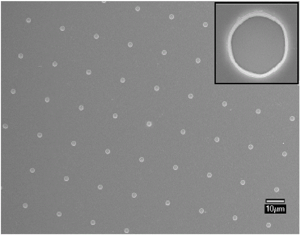
[0027] S1, preparation of conductive array substrate: uniformly coat the photoresist on the conductor with a coating thickness of 1 μm, irradiate with 380nm ultraviolet light for 6s, and bake at 120°C for 30min to prepare an array with ordered conductive holes The conductive array substrate, the diameter of the conductive hole is 5 μm, and the hole spacing is 20 μm;
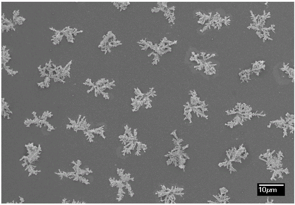
[0028] S2, preparation of ordered arrays of silver nanodendrites: In a standard three-electrode electrolytic cell, the conductive array substrate prepared in S1 was used as the working electrode, the platinum sheet was used as the counter electrode, and Ag / AgCl sealed in a saturated KCl solution was used as the The reference electrode, silver nitrate and surfactant CTAB are used as the electrolyte, the dosage of CTAB is 1% of the molar concentration of the silver nitrate solution, and the control voltage is -0.8~0.2V. Silver nano dendrites are deposited, and the electrodeposition time is 5 minutes to 2 hours. Aft...
Embodiment 2
[0031] S1, preparation of conductive array substrate: uniformly coat the photoresist on the conductor with a coating thickness of 2 μm, irradiate with 220nm ultraviolet light for 3s, and bake at 70°C for 50min to obtain ordered conductive holes The conductive array substrate of the array has a conductive hole diameter of 2 μm and a hole spacing of 10 μm.
[0032] S2, preparation of ordered arrays of gold nanodendrites: in a standard three-electrode electrolytic cell, the conductive array substrate prepared in S1 was used as the working electrode, the platinum sheet was used as the counter electrode, and Ag / AgCl sealed in a saturated KCl solution was used as the The reference electrode, the chloroauric acid solution and the surfactant SDS are used as the electrolyte, the amount of SDS is 0.5% of the molar concentration of the chloroauric acid solution, and the control voltage is -1 to 0.5V. Controllable electrodeposition of gold nanodendrites, the electrodeposition time is 10 m...
Embodiment 3
[0035] S1, preparation of conductive array substrate: uniformly coat the photoresist on the conductor with a coating thickness of 0.5 μm, irradiate with 300nm ultraviolet light for 4 minutes, and bake at 90°C for 10 minutes to obtain an ordered conductive substrate. The conductive array substrate of the hole array, the diameter of the conductive holes is 2.5 μm, and the hole spacing is 15 μm.
[0036] S2, preparation of copper nanodendrite ordered array: In a standard three-electrode electrolytic cell, the conductive array substrate prepared in S1 was used as the working electrode, the platinum sheet was used as the counter electrode, and Ag / AgCl sealed in a saturated KCl solution was used as the Reference electrode, copper acetate and complexing agent EDTA as the electrolyte, the amount of EDTA is 0.2% of the molar concentration of the copper acetate solution, the control voltage is -3 ~ -0.2V, and the surface of the conductive array substrate can be controlled by voltammetry ...
PUM
| Property | Measurement | Unit |
|---|---|---|
| diameter | aaaaa | aaaaa |
| size | aaaaa | aaaaa |
| size | aaaaa | aaaaa |
Abstract
Description
Claims
Application Information
 - Generate Ideas
- Intellectual Property
- Life Sciences
- Materials
- Tech Scout
- Unparalleled Data Quality
- Higher Quality Content
- 60% Fewer Hallucinations
Browse by: Latest US Patents, China's latest patents, Technical Efficacy Thesaurus, Application Domain, Technology Topic, Popular Technical Reports.
© 2025 PatSnap. All rights reserved.Legal|Privacy policy|Modern Slavery Act Transparency Statement|Sitemap|About US| Contact US: help@patsnap.com


