Copper Alloy Thin Wire for Ball Bonding

A copper alloy, thin wire technology, used in semiconductor/solid-state device parts, semiconductor devices, electrical components, etc., can solve the problems of unstable mechanical properties of thin bonding wires, unsolved tail bending wire front end bending, etc., and achieve delay The effect of copper alloy thin wire oxidation, stable spark discharge and uniform melting of solder balls

Active Publication Date: 2020-09-29
TANAKA DENSHI KOGYO KK
View PDF17 Cites 0 Cited by
  • Summary
  • Abstract
  • Description
  • Claims
  • Application Information

AI Technical Summary

Problems solved by technology

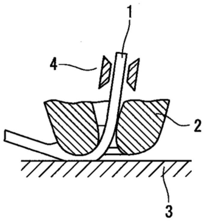
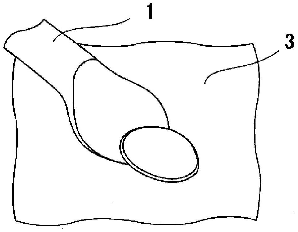
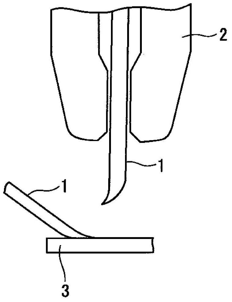
However, if only a concentrated layer of phosphorus (P) is provided on the surface of the bonding wire, the mechanical properties of the thin bonding wire itself become unstable, and the above-mentioned problems of tail wire bending or wire leading end bending are not solved.

Method used


Image

  • Copper Alloy Thin Wire for Ball Bonding
  • Copper Alloy Thin Wire for Ball Bonding
  • Copper Alloy Thin Wire for Ball Bonding

Examples


Embodiment

[0069] The core material uses copper (Cu) with a purity of 99.9998% by mass (5N), and phosphorus (P) and nickel (Ni), palladium (Pd), platinum (Pt), gold (Au) and silver (Ag) as an added element. As the base metal element, an element generally contained in high-purity copper is selected. That is, bismuth (Bi), selenium (Se), tellurium (Te), zinc (Zn), iron (Fe), nickel (Ni), and tin (Sn) are appropriately selected. These metals will be blended within a predetermined range as Example 1-Example 23. The details are shown in Table 1.

[0070] Next, this was subjected to continuous casting, and then the first wire drawing was performed to obtain a thick wire (diameter: 1.0 mm) before being covered with a stretching material. Next, intermediate heat treatment (400 degreeC x 4 hours) was performed. Afterwards, a noble metal coating layer formed by a gold (Au) thin extension layer and a palladium (Pd) extension layer is provided as required. The semi-finished wires were continuou...


PUM

PropertyMeasurementUnit
diameteraaaaaaaaaa

Abstract

The present invention provides a thin copper alloy wire for ball bonding, which is composed of the following components: nickel (Ni) is 0.02 mass % to 2 mass %, phosphorus (P) is 5 mass ppm to 800 mass ppm, The total amount of other base metal elements is less than 100 mass ppm and the remainder is copper (Cu).

Description

technical field [0001] The present invention relates to a thin copper alloy wire for ball bonding, which is suitable for connecting IC chip electrodes used in semiconductor devices to substrates such as external lead frames, and particularly relates to an extremely fine wire with a wire diameter of 15 μm or less , The copper alloy thin wire that does not bend the tail wire. Background technique [0002] In general, the first bonding of copper bonding wires and electrodes is performed using a method called ball bonding, and the wedge bonding of copper bonding wires and wiring on a circuit wiring board for semiconductors is performed using a method called wedge bonding. join. The first bonding is to apply a thermal arc from a torch electrode to the front end of the wire in the form of electronic frame off (EFO), so that the front end of the wire forms a positive ball called a solder ball (FAB). Next, ultrasonic waves (ultrasonic waves) are applied while pressing this FAB ont...

Claims


Application Information

Patent Timeline
Patent Type & Authority Patents(China)
IPC IPC(8): H01L23/49
CPCH01L24/45H01L2224/45147H01L2224/78301H01L2924/00011H01L2224/45015H01L2224/45565H01L2224/45572H01L2224/48456H01L2224/43848H01L2924/01028H01L2924/01015H01L2224/45664H01L2924/20751H01L2924/01004H01L2924/01079H01L2924/01047H01L2224/45644H01L2924/01046H01L2924/01078H01L2924/01026H01L2924/0103H01L2924/01034H01L2924/0105H01L2924/01052H01L2924/01083H01L2924/01205H01L2924/01206
Inventor 天野裕之
Owner TANAKA DENSHI KOGYO KK
Why Eureka
Try Eureka