Organic compound and use thereof
An organic compound and compound technology, applied in the field of organic electroluminescent materials, can solve problems such as increasing the economic cost of enterprises, and achieve the effects of reducing economic cost, improving optoelectronic performance, and reducing concentration quenching effect
- Summary
- Abstract
- Description
- Claims
- Application Information
AI Technical Summary
Problems solved by technology
Method used
Image

Examples
Embodiment 1-5
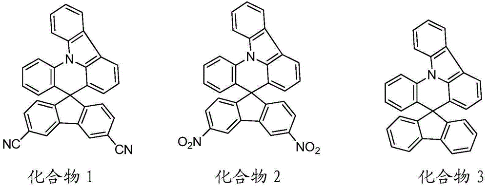
[0025] Embodiment 1-5 synthetic compound 1-5
[0026]
[0027] At -78°C, carbazole bromide (18.5mmol) was dissolved in dry tetrahydrofuran, then a solution of n-BuLi (1.6M dissolved in n-hexane, 11.2mL, 18.5mmol) was added thereto, and the reaction was stirred at low temperature for 3h . The above reaction solution was added to a tetrahydrofuran solution of 9-fluorenone derivatives and stirred at room temperature for 24 h. The reaction solution was extracted with ethyl acetate, MgSO 4 Dry, filter and concentrate the resulting reaction without further purification.
[0028] The above unpurified reactant (14.8mmol), glacial acetic acid (100mL) and concentrated HCl (3.0mL) were reacted at 130°C for 5h. After stopping the reaction, the residue was washed several times with methanol and water, and the target product was obtained by column chromatography.
[0029]
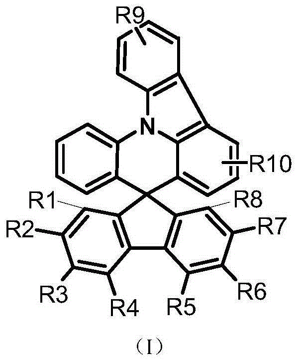
[0030] In the general structural formula (I), R1, R2, R4, R5, R7, R8, R9, and R10 are all hydrogen, and R3 a...
Embodiment 6
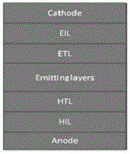
[0049] Embodiment 6 uses compound 5 to prepare organic electroluminescent device, and the device structure is as follows figure 1 shown.
[0050] The specific device structure and thickness are shown in Table 1 below.
[0051] Table 1 Device Structure and Thickness
[0052]
[0053] Among them, Anode: anode, HIL: hole injection layer, HTL: hole transport layer, Emitt inglayers (EML): light emitting layer, ETL: electron transport layer, EIL: electron injection layer, Cathode: cathode.
[0054] Device fabrication method: firstly, HAT-CN and NPB are sequentially deposited on the transparent conductive film ITO, the light-emitting layer adopts dual-source co-evaporation of DSA and compound 5 (L5), the doping concentration of L5 is 5% (mass percentage concentration), and the electron transport The layer adopts dual-source co-evaporation of Alq3 and LiQ, then evaporates LiF, and finally evaporates the cathode Al; during the completion of a device preparation process, the vacuum...
PUM
 Abstract
Description
Claims
Application Information
 - R&D
- Intellectual Property
- Life Sciences
- Materials
- Tech Scout
- Unparalleled Data Quality
- Higher Quality Content
- 60% Fewer Hallucinations
Browse by: Latest US Patents, China's latest patents, Technical Efficacy Thesaurus, Application Domain, Technology Topic, Popular Technical Reports.
© 2025 PatSnap. All rights reserved.Legal|Privacy policy|Modern Slavery Act Transparency Statement|Sitemap|About US| Contact US: help@patsnap.com