White-light OLED (organic light emission diode) device and preparation method thereof
An electroluminescent device and blue light emitting layer technology, applied in circuits, electrical components, electrical solid devices, etc., can solve the problem of difficult white light emission and the like, and achieve a light-color stability suitable for industrialized large-scale use, simple preparation process, etc. Effect
- Summary
- Abstract
- Description
- Claims
- Application Information
AI Technical Summary
Problems solved by technology
Method used
Image
Examples
Embodiment 1
[0041] A method for preparing a white light organic electroluminescence device, comprising the following steps:
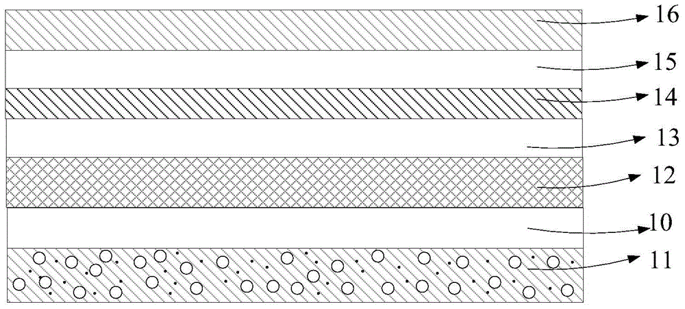
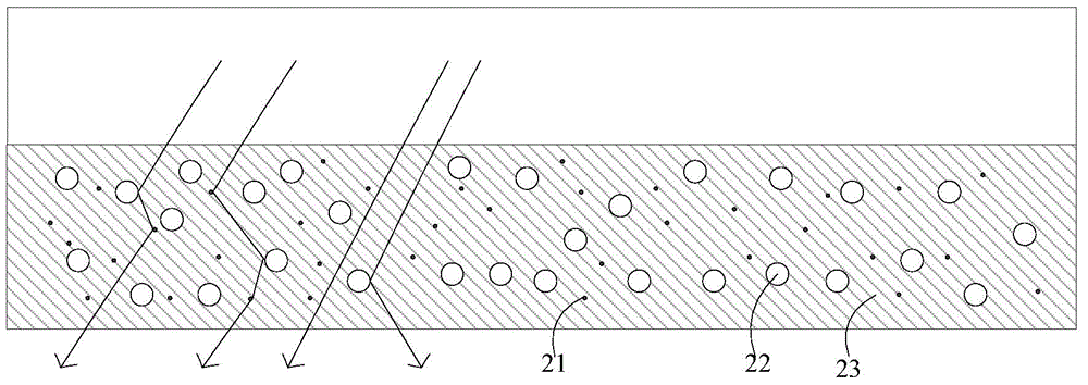
[0042] (1) Provide an ITO conductive glass with a sheet resistance of 5Ω / □ and clean it; prepare a red color conversion layer with a thickness of 80 μm on the side of the ITO conductive glass that is not covered with the ITO film (that is, the side of the glass substrate facing the air). DCM is dissolved with solvent dichloromethane to obtain a solution with a mass concentration of 20%, and then the resulting solution is added to the polyacrylate light-curing adhesive, and ceramic nano-titanium dioxide particles are added at the same time. The particle size of the titanium dioxide particles is 500nm. DCM and The mass ratio of polyacrylate is 0.2:100, the mass ratio of nano-titanium dioxide particles to polyacrylate is 5:100, and the dispersion and stirring are continued for 0.5 hours to obtain a mixed slurry. Then use screen printing technology to coat the mixed sl...
Embodiment 2
[0051] A method for preparing a white light organic electroluminescence device, comprising the following steps:
[0052] (1) Provide ITO conductive glass with a sheet resistance of 100Ω / □ and clean it; prepare a red light color conversion layer with a thickness of 20 μm on the side of the ITO conductive glass that is not covered with the ITO film (that is, the side of the glass substrate facing the air). Specifically, DCM is dissolved with dichloromethane as a solvent to obtain a solution with a mass concentration of 20%, and then the resulting solution is added to the polyacrylate light-curing adhesive, and ceramic nano-silica particles are added at the same time. The particle size is 50nm, the mass ratio of DCM to polyacrylate is 2:100, and the mass ratio of silicon dioxide to polyacrylate is 40:100, and the dispersion and stirring are continued for 1 hour to obtain a mixed slurry. Then use screen printing technology to coat the mixed slurry on the side of the conductive gla...
Embodiment 3
[0059] A method for preparing a white light organic electroluminescence device, comprising the following steps:
[0060] (1) Provide ITO conductive glass with a sheet resistance of 20Ω / □, and clean it; prepare a red color conversion layer with a thickness of 50 μm on the side of the ITO conductive glass that is not covered with the ITO film (that is, the side of the glass substrate facing the air). Specifically, DCM is dissolved with dichloromethane as a solvent to obtain a solution with a mass concentration of 20%, and then the resulting solution is added to the epoxy resin photocuring adhesive, and ceramic nano-silica particles are added at the same time. The particle size is 100nm, the mass ratio of DCM to epoxy resin is 1:100, and the mass ratio of silicon dioxide to epoxy resin is 20:100, and the mixed slurry is obtained by continuous dispersion and stirring for 0.8 hours. Then use screen printing technology to coat the mixed slurry on the side of the conductive glass tha...
PUM
 Abstract
Description
Claims
Application Information
 - R&D
- Intellectual Property
- Life Sciences
- Materials
- Tech Scout
- Unparalleled Data Quality
- Higher Quality Content
- 60% Fewer Hallucinations
Browse by: Latest US Patents, China's latest patents, Technical Efficacy Thesaurus, Application Domain, Technology Topic, Popular Technical Reports.
© 2025 PatSnap. All rights reserved.Legal|Privacy policy|Modern Slavery Act Transparency Statement|Sitemap|About US| Contact US: help@patsnap.com


