Optical assembly and display device
A technology of optical components and gratings, applied in optical components, optics, instruments, etc., can solve the problem of reducing the efficiency of optical waveguides, and achieve the effects of steep spectral characteristics, easy adjustment of light color, and improved color purity.
- Summary
- Abstract
- Description
- Claims
- Application Information
AI Technical Summary
Problems solved by technology
Method used
Image
Examples
Embodiment 1
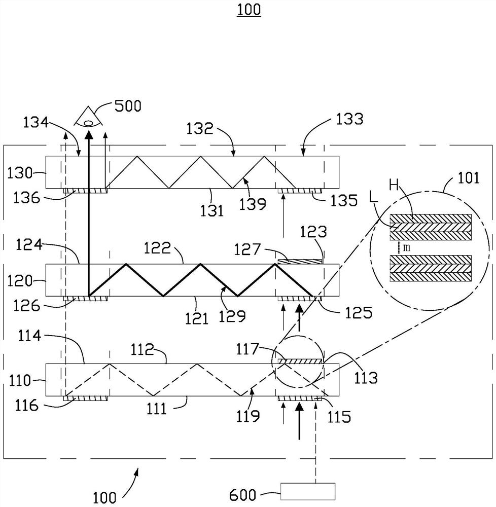
[0059] see figure 1 , this embodiment provides an optical assembly 100 . The optical assembly 100 includes a first transparent substrate 110 , a second transparent substrate 120 and a third transparent substrate 130 . The first light-transmitting substrate 110 is used to transmit the light 119 of the first wavelength band; the second light-transmitting substrate 120 is used to transmit the light 129 of the second wavelength band; the third light-transmitting substrate 130 is used to transmit the third wavelength band of light 139. The first waveband, the second waveband and the third waveband do not overlap each other. The material of the first transparent substrate 110 , the second transparent substrate 120 and the third transparent substrate 130 is, for example, glass.
[0060]The first light-transmitting substrate 110 includes a first surface 111 and a second surface 112 opposite to each other, and the second surface 112 includes a first light emitting area 113 and a sec...
Embodiment 2
[0071] see Figure 4 In this embodiment, an optical assembly 200 is provided. The optical assembly 200 includes a first transparent substrate 210 , a second transparent substrate 220 and a third transparent substrate 230 . The first light-transmitting substrate 210 includes a first surface 211 and a second surface 212 opposite to each other, and the second surface 212 includes a first light emitting area 213 and a second light emitting area 214 arranged at intervals. The second light-transmitting substrate 220 includes a third surface 221 and a fourth surface 222 opposite to each other, and the fourth surface 222 includes a third light emitting area 223 and a fourth light emitting area 224 arranged at intervals. The third light-transmitting substrate 230 includes a fifth surface 231 and a sixth surface 232 opposite to each other, and the sixth surface 232 includes a fifth light emitting area 233 and a sixth light emitting area 234 arranged at intervals.
[0072] The differenc...
Embodiment 3
[0081] see Figure 7 In this embodiment, an optical assembly 300 is provided, which includes a first transparent substrate 310 , a second transparent substrate 320 and a third transparent substrate 330 . The first light-transmitting substrate 310 includes a first surface 311 and a second surface 312 opposite to each other, and the second surface 312 includes a first light emitting area 313 and a second light emitting area 314 arranged at intervals. A first coupling-in grating 315 and a first coupling-out grating 316 are disposed on the first surface 311 at intervals. The first light emitting area 313 is provided with a first filter film 317 . The second light-transmitting substrate 320 includes a third surface 321 and a fourth surface 322 opposite to each other, and the fourth surface 322 includes a third light emitting area 323 and a fourth light emitting area 324 arranged at intervals. A second coupling-in grating 325 and a second coupling-out grating 326 are disposed on t...
PUM
| Property | Measurement | Unit |
|---|---|---|
| transmittivity | aaaaa | aaaaa |
| transmittivity | aaaaa | aaaaa |
| transmittivity | aaaaa | aaaaa |
Abstract
Description
Claims
Application Information
 - R&D
- Intellectual Property
- Life Sciences
- Materials
- Tech Scout
- Unparalleled Data Quality
- Higher Quality Content
- 60% Fewer Hallucinations
Browse by: Latest US Patents, China's latest patents, Technical Efficacy Thesaurus, Application Domain, Technology Topic, Popular Technical Reports.
© 2025 PatSnap. All rights reserved.Legal|Privacy policy|Modern Slavery Act Transparency Statement|Sitemap|About US| Contact US: help@patsnap.com


