THz modulator based on graphene-metal composite microstructure and preparation thereof
A metal microstructure and metal composite technology, which is applied in the fields of instruments, semiconductor/solid-state device manufacturing, and optics, can solve the problems of quality factor, adjustable performance, and modulation depth, etc., and achieve large modulation depth and large modulation depth , good effect of adjustable performance
- Summary
- Abstract
- Description
- Claims
- Application Information
AI Technical Summary
Problems solved by technology
Method used
Image
Examples
Embodiment 1
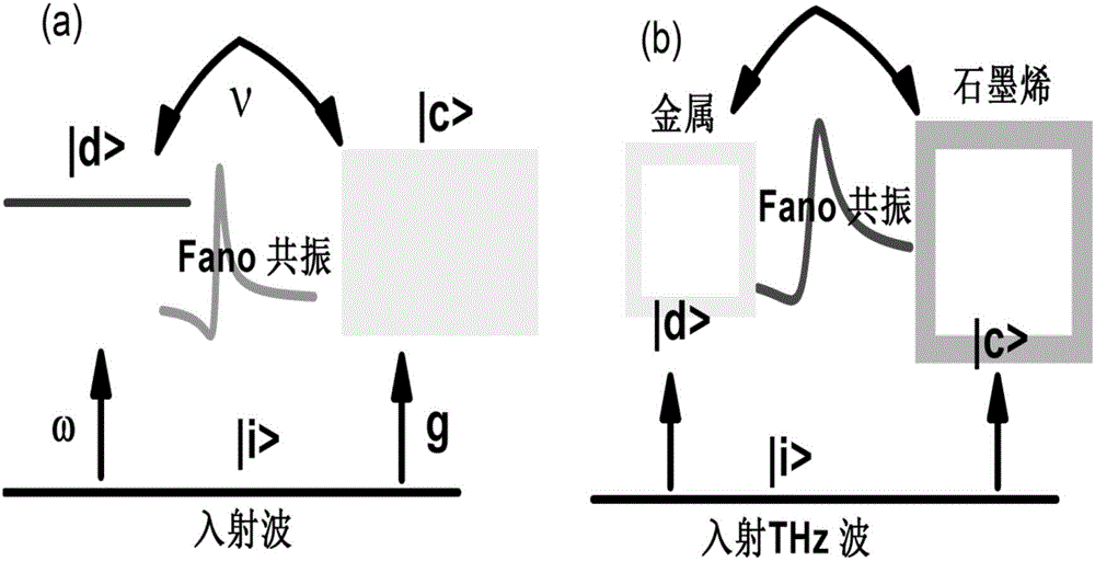
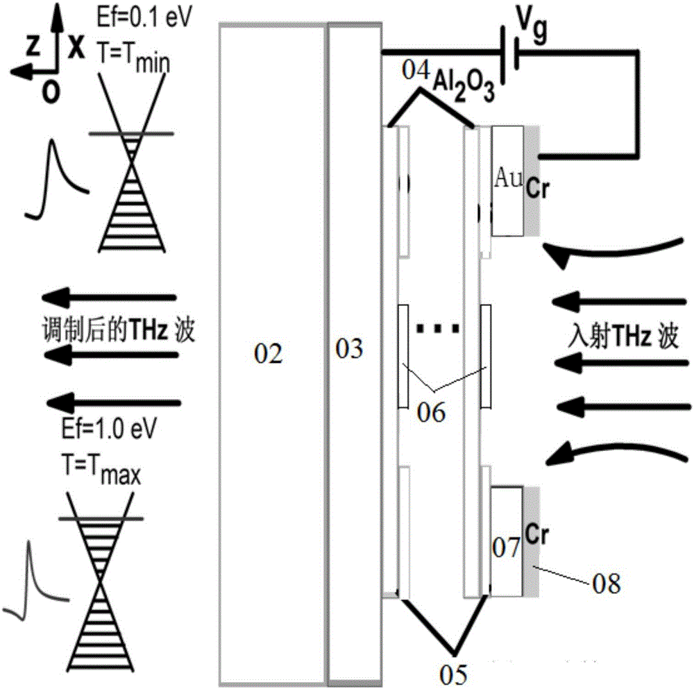
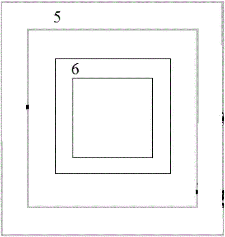
[0058] see Figure 1 to Figure 5 As shown, the THz modulator of the graphene-metal composite microstructure is fabricated by the following steps:
[0059] (1) Fabrication of polymer flexible substrate layer 02: ordinary Si sheet is used as sacrificial layer 01, and the solution containing plastic polymer flexible substrate layer 02 is sprayed on it by spincoating method, and then dried in an oven About 30 minutes, the temperature range is 150-200 degrees, and then use a high-temperature furnace in an inert gas (or N 2 ) in a protective atmosphere to 300-400 (preferably 350 degrees), forming a uniform polymer flexible substrate layer 02 thin layer;
[0060] (2) Making an epitaxial layer doped with Si: form a doped semiconductor epitaxial layer 03 with a thickness of 1-10 μm by epitaxial growth method, and the doping concentration is 3×10 16 cm -3 , the electrical conductivity of the Si layer is 1-10Ω·cm, and the insulation is good, so as to reduce the loss;
[0061] (3) For...
Embodiment 2
[0082] The preparation method of the THz modulator based on the graphene-metal composite microstructure comprises the following steps:
[0083] (1) Making polymer flexible substrate layer
[0084] Using ordinary Si as a sacrificial layer, spray a solution containing a plastic flexible substrate on the sacrificial layer, dry it at 150°C for 40 minutes, and then heat it to 400°C under the protection of an inert gas for curing to obtain a polymer with a thickness of 1 μm. Flexible substrate layer;
[0085] (2) Fabrication of doped semiconductor epitaxial layer
[0086] A doped Si layer with a thickness of 1 μm was formed by epitaxial growth method, and the doping concentration was 10 15 cm -3 , the conductivity of the Si layer is 1Ω·cm;
[0087] (3) Making Al 2 o 3 Insulation-active region structure composite layer
[0088] (3-1) Atomic layer deposition of Al on doped semiconductor epitaxial layer 2 o 3 , formed at a temperature of 200 °C, and then rinsed with distilled ...
Embodiment 3
[0096] The preparation method of the THz modulator based on the graphene-metal composite microstructure comprises the following steps:
[0097] (1) Making polymer flexible substrate layer
[0098] Using ordinary Si as a sacrificial layer, spray a solution containing a plastic flexible substrate on the sacrificial layer, dry it at 200°C for 20 minutes, and then heat it to 300°C under the protection of an inert gas for curing to obtain a polymer with a thickness of 50 μm. Flexible substrate layer;
[0099] (2) Fabrication of doped semiconductor epitaxial layer
[0100] A doped Si layer with a thickness of 10 μm was formed by epitaxial growth method, and the doping concentration was 10 18 cm -3 , the electrical conductivity of the Si layer is 10Ω·cm;
[0101] (3) Making Al 2 o 3 Insulation-active region structure composite layer
[0102] (3-1) Atomic layer deposition of Al on doped semiconductor epitaxial layer 2 o 3 , formed at a temperature of 200 degrees Celsius, and ...
PUM
| Property | Measurement | Unit |
|---|---|---|
| thickness | aaaaa | aaaaa |
| thickness | aaaaa | aaaaa |
| thickness | aaaaa | aaaaa |
Abstract
Description
Claims
Application Information
 - Generate Ideas
- Intellectual Property
- Life Sciences
- Materials
- Tech Scout
- Unparalleled Data Quality
- Higher Quality Content
- 60% Fewer Hallucinations
Browse by: Latest US Patents, China's latest patents, Technical Efficacy Thesaurus, Application Domain, Technology Topic, Popular Technical Reports.
© 2025 PatSnap. All rights reserved.Legal|Privacy policy|Modern Slavery Act Transparency Statement|Sitemap|About US| Contact US: help@patsnap.com


