An organic solar cell that constructs an internal electric field by doping nanoparticles in a charge transport layer and its preparation method
A charge transport layer and solar cell technology, applied in organic semiconductor devices, circuits, photovoltaic power generation, etc., can solve the problems of low device performance and low carrier transfer efficiency, achieve high photoelectric conversion capability, improve mobility, and cost performance high effect
- Summary
- Abstract
- Description
- Claims
- Application Information
AI Technical Summary
Problems solved by technology
Method used
Image
Examples
Embodiment 1
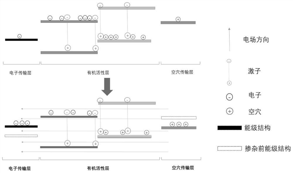
[0033] An organic solar cell that builds an internal electric field by doping nanoparticles in the charge transport layer, such as figure 1 As shown, it includes a substrate, the substrate has an electrode layer, the electrode layer is plated with an electron transport layer doped with P-type semiconductor nanoparticles, and the electron transport layer doped with P-type semiconductor nanoparticles is spin-coated from bottom to top An organic functional layer and a hole transport layer doped with N-type semiconductor nanoparticles are provided, and a metal electrode layer is plated on the hole transport layer doped with N-type semiconductor nanoparticles.
[0034] Wherein, the substrate is a glass substrate.
[0035] The electrode layer adopts the ITO transparent conductive electrode on the glass substrate.
[0036] The electron transport layer doped with P-type semiconductor nanoparticles adopts a ZnO film with a thickness of 10 nm doped with 2wt% Cu2O nanoparticles.
[003...
Embodiment 2
[0047] Example 2: Comparative Example
[0048] On the basis of Embodiment 1, the difference between this embodiment and Embodiment 1 is that the electron transport layer and the hole transport layer are not doped, which is not enough to build the internal electric field of the device. Solar cells, and Example 1 constitute a control group.
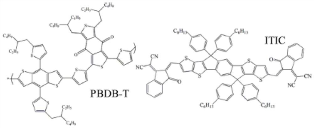
[0049] The glass substrate is used as the substrate, the ITO electrode is used for the electrode layer, ZnO is used for the electron transport layer, the PBDB-T:ITIC bulk heterojunction is used for the organic functional layer, the MnO3 is used for the hole transport layer, and the silver electrode is used for the electrode layer 6.
[0050] The specific preparation method is as follows:
[0051] 1. Cleaning the substrate: Put the glass substrate with the conductive electrode 2 into detergent, acetone, deionized water, and isopropanol in sequence, ultrasonically clean for 15 minutes each time, and then dry it with an inert gas and oxidize ...
PUM
| Property | Measurement | Unit |
|---|---|---|
| thickness | aaaaa | aaaaa |
| thickness | aaaaa | aaaaa |
| thickness | aaaaa | aaaaa |
Abstract
Description
Claims
Application Information
 - Generate Ideas
- Intellectual Property
- Life Sciences
- Materials
- Tech Scout
- Unparalleled Data Quality
- Higher Quality Content
- 60% Fewer Hallucinations
Browse by: Latest US Patents, China's latest patents, Technical Efficacy Thesaurus, Application Domain, Technology Topic, Popular Technical Reports.
© 2025 PatSnap. All rights reserved.Legal|Privacy policy|Modern Slavery Act Transparency Statement|Sitemap|About US| Contact US: help@patsnap.com


