A kind of solar cell and its passivation contact structure, battery module and photovoltaic system
A technology of solar cells and contact structures, applied in the field of solar cells, can solve the problems of poor isolation effect of conductive layers, increased recombination, decreased conversion efficiency, etc., and achieves the effects of increasing interface defects, enhancing gettering effect, and reducing sensitivity
- Summary
- Abstract
- Description
- Claims
- Application Information
AI Technical Summary
Problems solved by technology
Method used
Image
Examples
Embodiment 1
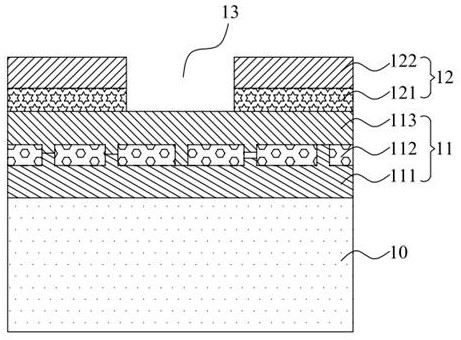
[0077] The embodiment of the present invention provides a passivation contact structure of a solar cell. For the convenience of description, only the parts related to the embodiment of the present invention are shown. Refer to figure 1 As shown, the passivation contact structure of the solar cell provided by the embodiment of the present invention includes:
[0078] a first passivation contact region 11 disposed on the silicon substrate 10, and a second passivation contact region 12 disposed on the first passivation contact region 11;
[0079] The second passivation contact region 12 has an opening 13, so that the conductive layer is connected to the first passivation contact region 11 through the opening 13;
[0080] The first passivation contact region 11 includes a first doped layer 111, a first passivation layer 112, and a second doped layer 113, and the second passivation contact region 12 includes a second passivation layer 121, and a third doped layer 113. Layer 122. ...
Embodiment 2
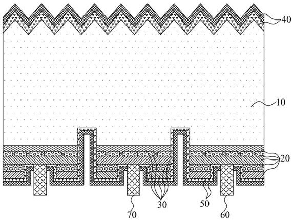
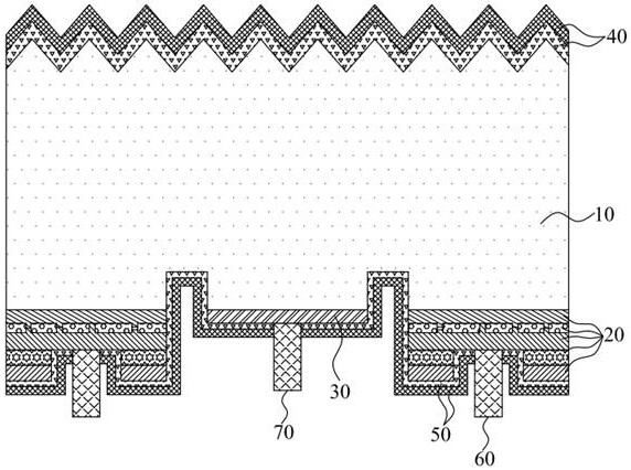
[0096] The second embodiment of the present invention provides a solar cell. For the convenience of description, only the parts related to the embodiment of the present invention are shown. Refer to Figure 2-Figure 11 As shown, the solar cell provided by the embodiment of the present invention includes:
[0097] silicon substrate 10;
[0098] The first doped region 20 and the second doped region 30 arranged at intervals on the back of the silicon substrate 10, the polarity of the first doped region 20 and the second doped region 30 are opposite;
[0099] a first dielectric layer 40 disposed on the front side of the silicon substrate 10;
[0100] a second dielectric layer 50 disposed between the first doped region 20 and the second doped region 30; and
[0101] a first conductive layer 60 disposed on the first doped region 20 and a second conductive layer 70 disposed on the second doped region 30;
[0102] Wherein, the first doped region 20 and / or the second doped region 30...
Embodiment 3
[0146] The third embodiment of the present invention provides a solar cell. For the convenience of description, only the parts related to the embodiment of the present invention are shown. Refer to Figure 12 As shown, the solar cell provided by the embodiment of the present invention includes:
[0147] silicon substrate 10;
[0148] The passivation contact structure 1 as described in the previous embodiment is arranged on the back side of the silicon substrate 10;
[0149] a third dielectric layer 80 disposed on the passivation contact structure 1;
[0150] a sixth doped layer 90 and a fourth dielectric layer 100 sequentially disposed on the front surface of the silicon substrate 10; and
[0151] a third conductive layer 110 electrically connected to the passivation contact structure 1 and a fourth conductive layer 120 electrically connected to the sixth doped layer 90;
[0152] Wherein the polarity of the passivation contact structure 1 is opposite to that of the sixth do...
PUM
| Property | Measurement | Unit |
|---|---|---|
| thickness | aaaaa | aaaaa |
| thickness | aaaaa | aaaaa |
| thickness | aaaaa | aaaaa |
Abstract
Description
Claims
Application Information
 - Generate Ideas
- Intellectual Property
- Life Sciences
- Materials
- Tech Scout
- Unparalleled Data Quality
- Higher Quality Content
- 60% Fewer Hallucinations
Browse by: Latest US Patents, China's latest patents, Technical Efficacy Thesaurus, Application Domain, Technology Topic, Popular Technical Reports.
© 2025 PatSnap. All rights reserved.Legal|Privacy policy|Modern Slavery Act Transparency Statement|Sitemap|About US| Contact US: help@patsnap.com


